XRP6275 3A Ultra Low Dropout Voltage Regulator January 2015
Rev. 2.0.0
GENERAL DESCRIPTION
FEATURES
The XRP6275 is an ultra a low dropout voltage regulator capable of delivering 3A output currents. It is unique in the industry in being able to operate from a single supply rail of 1.045V to 2.625V without the need for a noise generating charge pump.
• 3A Output Current
With its ultra low dropout voltage of 138 138mV at full load guaranteed over temperature, the XRP6275 achieves conversions onversions previously unavailable. The output voltage can be set as low as 0.6V with ±0.5% accuracy making the XRP6275 perfectly suited for powering low voltage devices such as FPGAs, DSPs, ASICs, and other SOCs. Built-in in current limit, reverse bias and thermal protection ensures safe operation under abnormal operating conditions. An enable function, soft start and Power Good flag complete the feature set. The XRP6275 is offered in RoHS compliant, “green”/halogen free 10-pin pin 3x3mm DFN package.
• 1.045V to 2.625V V Single Input Voltage − Adjustable Output Voltage ≥0.6V − ±0.5 Output Voltage Accuracy • Ultra Low Dropout Voltage − 138mV mV Max over temp @ 3A 3 − 74mV Max over temp @ 2A • Power Good Flag • Enable & Soft Start • Current Limit and Thermal Protection • Reverse Bias Protection • RoHS compliant “Green”/Halogen Free − 10-pin pin 3mm x 3mm DFN
APPLICATIONS • Point of Load Conversion • Microprocessors, DSPs, FPGAs Supplies • Networking & Telecom Equipment • Switching Supplies Post Regulation
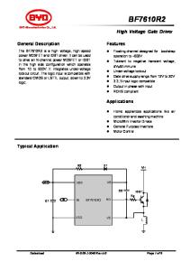
TYPICAL APPLICATION DIAGRAM
XRP6275
Fig. 1: XRP6275 Application Diagram
Exar Corporation 48720 Kato Road, Fremont CA 94538, USA
www.exar.com Tel. +1 510 668-7000 – Fax. +1 510 668-7001 668
XRP6275 3A Ultra Low Dropout Voltage Regulator ABSOLUTE MAXIMUM RATINGS INGS
OPERATING RATINGS
These are stress ratings only and functional operation of the device at these ratings or above any other of those indicated in the operation sections of the specifications below is not implied. Exposure to absolute maximum rating conditions for extended periods of time may affect reliability.
Input Voltage Range VIN, VEN, VPGOOD ........... 1.045V-2.625V Junction Temperature Range ....................-40°C to 125°C Thermal Resistance ΘJC DFN10 .............................. 6°C/W Thermal Resistance ΘJA DFN10 ..........................40.5°C/W ..........................
Input Voltage VIN, VPGOOD ................................ ............................................ 3V Enable Voltage VEN .................................... .... VIN+0.5V≤3V Storage Temperature .............................. -65°C to 150°C Junction Temperature ................................ .......................................... 150°C Lead Temperature (Soldering, 5 sec) ..................... 260°C ESD Rating (HBM - Human Body Model) .................... 2kV ESD Rating (CDM – Charged Device Model) .............. 1kV
ELECTRICAL SPECIFICATIONS TIONS Specifications are for an Operating Junction Temperature of TJ = TA = 25°C only; limits applying over the full Operating Junction Temperature range are denoted by a ““•”. Typical values represent the most likely parametric norm at TJ = 25°C, and are provided for reference purposes only. Unless otherwise indicated, VIN = VOUT + 0.5V V and IOUT=20mA, CIN = 47µF, COUT = 47µF, TA= 25°C. Parameter
Min.
Input Voltage Operating Range
1.045
Maximum Output Current1
2.625
2.5 598.5 594.0 597.0 592.0 596.0 590.7
Power Supply Rejection Ratio (PSRR) Output Noise Voltage
Start Up time Power Good Threshold Power Good Threshold Hysteresis PGOOD Output Low
© 2015 Exar Corporation
92
mA
EN active
mA
EN active , IOUT=3A VEN=0V, IOUT=0mA, PGOOD Floating
604.5 606.0 603.0 605.0 602.0 604.0 138
µA mV mV mV mV mV mV mV
74
mV
0.25
%
VIN=VOUT + 0.5V, 20mA≤I 20mA OUT ≤3A
35
dB
f=1kHz
30
dB
f>300kHz
200
µVRMS
12 601.5 600.0 599.0
4.7
• • • • •
VIN=2.5V, VOUT>1V VIN=1.8V VIN=1.35V IOUT=3A, VOUT=1.0V (Note 2) IOUT=2A, VOUT=1.35V (Note 2)
10Hz-100kHz
A
VOUT = 0.9 × VOUT(NOM)
-10
µA
VIN=0V, VOUT=2.625V
160
°C
3.3
Thermal Shutdown Hysteresis
•
6.0
Output Voltage Load Regulation
Thermal Shutdown Temperature
V
Conditions
A
Dropout Voltage
Reverse Bias Protection VOUT Leakage current
Units
2.0
Shutdown Current
Current Limit
Max.
3
Ground Current
ADJ Pin Voltage
Typ.
30
°C
2
ms
94
97
2.8
% of VOUT
VOUT=1.0V •
VOUT rising VOUT falling
% of VOUT 0.4
V
•
VIN>1.5V, ISINK=1mA
0.4
V
•
VIN>1.045V, ISINK=100uA
2/11
Rev. 2.0.0
XRP6275 3A Ultra Low Dropout Voltage Regulator Parameter
Min.
Typ.
Max.
0.43
0.55
0.67
Units
Conditions
Enable Pin Specifications Enable Threshold Voltage EN Sink Current Maximum Allowable EN Sink Current EN Source Current
V
•
VEN rising
2.5
uA
EN