LTC6409 10GHz GBW, 1.1nV/√Hz Differential Amplifier/ADC Driver Description
Features 10GHz Gain-Bandwidth Product n 88dB SFDR at 100MHz, 2V P-P n 1.1nV/√Hz Input Noise Density n Input Range Includes Ground n External Resistors Set Gain (Min 1V/V) n 3300V/µs Differential Slew Rate n 52mA Supply Current n 2.7V to 5.25V Supply Voltage Range n Fully Differential Input and Output n Adjustable Output Common Mode Voltage n Low Power Shutdown n Small 10-Lead 3mm × 2mm × 0.75mm QFN Package
The LTC®6409 is a very high speed, low distortion, differential amplifier. Its input common mode range includes ground, so that a ground-referenced input signal can be DC-coupled, level-shifted, and converted to drive an ADC differentially.
n
The gain and feedback resistors are external, so that the exact gain and frequency response can be tailored to each application. For example, the amplifier could be externally compensated in a no-overshoot configuration, which is desired in certain time-domain applications. The LTC6409 is stable in a differential gain of 1. This allows for a low output noise in applications where gain is not desired. It draws 52mA of supply current and has a hardware shutdown feature which reduces current consumption to 100µA.
Applications n n n n n
Differential Pipeline ADC Driver High-Speed Data-Acquisition Cards Automated Test Equipment Time Domain Reflexometry Communications Receivers
The LTC6409 is available in a compact 3mm × 2mm 10‑pin leadless QFN package and operates over a –40°C to 125°C temperature range. L, LT, LTC, LTM, Linear Technology and the Linear logo are registered trademarks of Linear Technology Corporation. All other trademarks are the property of their respective owners.
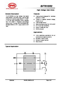
Typical Application DC-Coupled Interface from a Ground-Referenced Single-Ended Input to an LTC2262-14 ADC
LTC6409 Driving LTC2262-14 ADC, fIN = 70MHz, –1dBFS, fS = 150MHz, 4096-Point FFT
1.3pF VIN
150Ω
150Ω 1.8V
– + VOCM = 0.9V
LTC6409
+ –
33.2Ω
10Ω
33.2Ω
10Ω 39pF
150Ω
AIN+
VDD
LTC2262-14 ADC AIN–
GND
–60 –70 –80 –90 –100
150Ω 6409 TA01
1.3pF
AMPLITUDE (dBFS)
39pF
3.3V
0 VS = 3.3V –10 V OUTDIFF = 1.8VP-P –20 HD2 = –86.5dBc HD3 = –89.4dBc –30 SFDR = 81.6dB –40 SNR = 71.1dB –50
–110 –120
0
10
20
30 40 50 FREQUENCY (MHz)
60
70 6409 TA01b
6409fa
1
LTC6409 Absolute Maximum Ratings
Pin Configuration
(Note 1)
2
V+
V–
9
8
11,V– 3
4
5 VOCM
+IN
10
V+
1
SHDN
–OUT
V–
TOP VIEW
Total Supply Voltage (V+ – V–)..................................5.5V Input Current (+IN, –IN, VOCM, SHDN) (Note 2)................................................................. ±10mA Output Short-Circuit Duration (Note 3)............. Indefinite Operating Temperature Range (Note 4)................................................... –40°C to 125°C Specified Temperature Range (Note 5)................................................... –40°C to 125°C Maximum Junction Temperature........................... 150°C Storage Temperature Range................... –65°C to 150°C
7
+OUT
6
–IN
UDB PACKAGE 10-LEAD (3mm × 2mm) PLASTIC QFN TJMAX = 150°C, θJA = 138°C/W, θJC = 5.2°C/W EXPOSED PAD (PIN 11) CONNECTED TO V–
Order Information Lead Free Finish TAPE AND REEL (MINI)
TAPE AND REEL
PART MARKING*
PACKAGE DESCRIPTION
SPECIFIED TEMPERATURE RANGE
LTC6409CUDB#TRMPBF
LTC6409CUDB#TRPBF
LFPF
10-Lead (3mm × 2mm) Plastic QFN
0°C to 70°C
LTC6409IUDB#TRMPBF
LTC6409IUDB#TRPBF
LFPF
10-Lead (3mm × 2mm) Plastic QFN
–40°C to 85°C
LTC6409HUDB#TRMPBF
LTC6409HUDB#TRPBF LFPF 10-Lead (3mm × 2mm) Plastic QFN TRM = 500 pieces. *Temperature grades are identified by a label on the shipping container. Consult LTC Marketing for parts specified with wider operating temperature ranges. Consult LTC Marketing for information on lead based finish parts. For more information on lead free part marking, go to: http://www.linear.com/leadfree/ For more information on tape and reel specifications, go to: http://www.linear.com/tapeandreel/
–40°C to 125°C
Electrical Characteristics
The l denotes the specifications which apply over the full operating temperature range, otherwise specifications are at TA = 25°C. V+ = 5V, V– = 0V, VCM = VOCM = VICM = 1.25V, VSHDN = open. VS is defined as (V+ – V–). VOUTCM is defined as (V+OUT + V–OUT)/2. VICM is defined as (V+IN + V–IN)/2. VOUTDIFF is defined as (V+OUT – V–OUT). SYMBOL PARAMETER VOSDIFF
Differential Offset Voltage (Input Referred)
ΔVOSDIFF Differential Offset Voltage Drift (Input Referred) ΔT
CONDITIONS VS = 3V VS = 3V VS = 5V VS = 5V
MIN
TYP
MAX
UNITS
±300
±1000 ±1200 ±1100 ±1400
µV µV µV µV
l
±300 l
VS = 3V VS = 5V
l l
2 2 –140 –160
µV/°C µV/°C
IB
Input Bias Current (Note 6)
VS = 3V VS = 5V
l l
–62 –70
0 0
µA µA
IOS
Input Offset Current (Note 6)
VS = 3V VS = 5V
l l
±2 ±2
±10 ±10
µA µA
RIN
Input Resistance
Common Mode Differential Mode
165 860
CIN
Input Capacitance
Differential Mode
0.5
pF
en
Differential Input Noise Voltage Density
f = 1MHz, Not Including RI/RF Noise
1.1
nV/√Hz
in
Input Noise Current Density
f = 1MHz, Not Including RI/RF Noise
8.8
pA/√Hz
NF
Noise Figure at 100MHz
Shunt-Terminated to 50Ω, RS = 50Ω, RI = 25Ω, RF = 10kΩ
6.9
dB
kΩ Ω
6409fa
2
LTC6409 Electrical Characteristics The l denotes the specifications which apply over the full operating + –
temperature range, otherwise specifications are at TA = 25°C. V = 5V, V = 0V, VCM = VOCM = VICM = 1.25V, VSHDN = open. VS is defined as (V+ – V–). VOUTCM is defined as (V+OUT + V–OUT)/2. VICM is defined as (V+IN + V–IN)/2. VOUTDIFF is defined as (V+OUT – V–OUT). SYMBOL PARAMETER
CONDITIONS
MIN
TYP
MAX
enVOCM
Common Mode Noise Voltage Density
f = 10MHz
VICMR (Note 7)
Input Signal Common Mode Range
VS = 3V VS = 5V
l l
0 0
CMRRI (Note 8)
Input Common Mode Rejection Ratio (Input Referred) ΔVICM/ΔVOSDIFF
VS = 3V, VICM from 0V to 1.5V VS = 5V, VICM from 0V to 3.5V
l l
75 75
90 90
dB dB
VS = 3V, VOCM from 0.5V to 1.5V VS = 5V, VOCM from 0.5V to 3.5V
l l
55 60
80 85
dB dB
VS = 2.7V to 5.25V
l
60
85
dB
VS = 2.7V to 5.25V
l
55
70
dB
l
2.7
CMRRIO Output Common Mode Rejection Ratio (Input (Note 8) Referred) ΔVOCM/ΔVOSDIFF PSRR (Note 9)
Differential Power Supply Rejection (ΔVS/ΔVOSDIFF)
PSRRCM Output Common Mode Power Supply Rejection (Note 9) (ΔVS/ΔVOSCM) Supply Voltage Range (Note 10) VS
12
UNITS nV/√Hz
1.5 3.5
5.25
V V
V
GCM
Common Mode Gain (ΔVOUTCM/ΔVOCM)
VS = 3V, VOCM from 0.5V to 1.5V VS = 5V, VOCM from 0.5V to 3.5V
l l
1 1
ΔGCM
Common Mode Gain Error, 100 × (GCM – 1)
VS = 3V, VOCM from 0.5V to 1.5V VS = 5V, VOCM from 0.5V to 3.5V
l l
±0.1 ±0.1
±0.3 ±0.3
% %
BAL
Output Balance (ΔVOUTCM/ ΔVOUTDIFF)
ΔVOUTDIFF = 2V Single-Ended Input Differential Input
l l
–65 –70
–50 –50
dB dB
VOSCM
Common Mode Offset Voltage (VOUTCM – VOCM)
VS = 3V VS = 5V
l l
±1 ±1
±5 ±6
mV mV
∆VOSCM ∆T
Common Mode Offset Voltage Drift
l
4
VOUTCMR Output Signal Common Mode Range (Note 7) (Voltage Range for the VOCM Pin)
VS = 3V VS = 5V
RINVOCM Input Resistance, VOCM Pin
0.5 0.5
l
30
V V
40
50
KΩ
1.6
V V
l
0.9
0.85 1.25
Output Voltage, High, Either Output Pin
VS = 3V, IL = 0 VS = 3V, IL = –20mA VS = 5V, IL = 0 VS = 5V, IL = –20mA
l l l l
1.85 1.8 3.85 3.8
2 1.95 4 3.95
Output Voltage, Low, Either Output Pin
VS = 3V, 5V; IL = 0 VS = 3V, 5V; IL = 20mA
l l
ISC
Output Short-Circuit Current, Either Output Pin (Note 11)
VS = 3V VS = 5V
l l
AVOL
Large-Signal Open Loop Voltage Gain
IS
Supply Current
VOUT
0.06 0.2 ±50 ±70
µV/°C 1.5 3.5
VS = 3V, VOCM = Open VS = 5V, VOCM = Open
VOCM
Self-Biased Voltage at the VOCM Pin
l l
V/V V/V
V V V V 0.15 0.4
V V
±70 ±95
mA mA
65
dB
52 l
56 58
mA mA
ISHDN
Supply Current in Shutdown
VSHDN ≤ 0.6V
l
RSHDN
SHDN Pull-Up Resistor
VSHDN = 0V to 0.5V
l
VIL
SHDN Input Logic Low
l
VIH
SHDN Input Logic High
l
tON
Turn-On Time
160
ns
tOFF
Turn-Off Time
80
ns
115
100
500
µA
150
185
KΩ
0.6
V
1.4
V
6409fa
3
LTC6409 Electrical Characteristics The l denotes the specifications which apply over the full operating + –
temperature range, otherwise specifications are at TA = 25°C. V = 5V, V = 0V, VCM = VOCM = VICM = 1.25V, VSHDN = open. VS is defined as (V+ – V–). VOUTCM is defined as (V+OUT + V–OUT)/2. VICM is defined as (V+IN + V–IN)/2. VOUTDIFF is defined as (V+OUT – V–OUT). SYMBOL PARAMETER
CONDITIONS
MIN
SR
Slew Rate
Differential Output, VOUTDIFF = 4VP-P +OUT Rising (–OUT Falling) +OUT Falling (–OUT Rising)
GBW
Gain-Bandwidth Product
RI = 25Ω, RF = 10kΩ, fTEST = 100MHz l
9.5 8
TYP
MAX
UNITS
3300 1720 1580
V/µs V/µs V/µs
10
GHz GHz
f–3dB
–3dB Frequency
RI = RF = 150Ω, RLOAD = 400Ω, CF = 1.3pF
2
GHz
f0.1dB
Frequency for 0.1dB Flatness
RI = RF = 150Ω, RLOAD = 400Ω , CF = 1.3pF
600
MHz
FPBW
Full Power Bandwidth
VOUTDIFF = 2VP-P
550
MHz
HD2 HD3
25MHz Distortion
Differential Input, VOUTDIFF = 2VP-P, RI = RF = 150Ω, RLOAD = 400Ω 2nd Harmonic 3rd Harmonic
–104 –106
dBc dBc
Differential Input, VOUTDIFF = 2VP-P, RI = RF = 150Ω, RLOAD = 400Ω 2nd Harmonic 3rd Harmonic
–93 –88
dBc dBc
Single-Ended Input, VOUTDIFF = 2VP-P, RI = RF = 150Ω, RLOAD = 400Ω 2nd Harmonic 3rd Harmonic
–101 –103
dBc dBc
Single-Ended Input, VOUTDIFF = 2VP-P, RI = RF = 150Ω, RLOAD = 400Ω 2nd Harmonic 3rd Harmonic
–88 –93
dBc dBc
100MHz Distortion
HD2 HD3
25MHz Distortion
100MHz Distortion
IMD3
3rd Order IMD at 25MHz f1 = 24.9MHz, f2 = 25.1MHz
VOUTDIFF = 2VP-P Envelope, RI = RF = 150Ω, RLOAD = 400Ω
–110
dBc
3rd Order IMD at 100MHz f1 = 99.9MHz, f2 = 100.1MHz
VOUTDIFF = 2VP-P Envelope, RI = RF = 150Ω, RLOAD = 400Ω
–98
dBc
3rd Order IMD at 140MHz f1 = 139.9MHz, f2 = 140.1MHz
VOUTDIFF = 2VP-P Envelope, RI = RF = 150Ω, RLOAD = 400Ω
–88
dBc
59 53 48
dBm dBm dBm
1.9
ns
OIP3
Equivalent OIP3 at 25MHz (Note 12) Equivalent OIP3 at 100MHz (Note 12) Equivalent OIP3 at 140MHz (Note 12)
tS
Settling Time
VOUTDIFF = 2VP-P Step, RI = RF = 150Ω, RLOAD = 400Ω 1% Settling
Note 1: Stresses beyond those listed under Absolute Maximum Ratings may cause permanent damage to the device. Exposure to any Absolute Maximum Rating condition for extended periods may affect device reliability and lifetime. Note 2: Input pins (+IN, –IN, VOCM, and SHDN) are protected by steering diodes to either supply. If the inputs should exceed either supply voltage, the input current should be limited to less than 10mA. In addition, the inputs +IN, –IN are protected by a pair of back-to-back diodes. If the differential input voltage exceeds 1.4V, the input current should be limited to less than 10mA. Note 3: A heat sink may be required to keep the junction temperature below the absolute maximum rating when the output is shorted indefinitely.
Note 4: The LTC6409C/LTC6409I are guaranteed functional over the temperature range of –40°C to 85°C. The LTC6409H is guaranteed functional over the temperature range of –40°C to 125°C. Note 5: The LTC6409C is guaranteed to meet specified performance from 0°C to 70°C. The LTC6409C is designed, characterized and expected to meet specified performance from –40°C to 85°C, but is not tested or QA sampled at these temperatures. The LTC6409I is guaranteed to meet specified performance from –40°C to 85°C. The LTC6409H is guaranteed to meet specified performance from –40°C to 125°C. Note 6: Input bias current is defined as the average of the input currents flowing into the inputs (–IN and +IN). Input offset current is defined as the difference between the input currents (IOS = IB+ – IB–).
6409fa
4
LTC6409 Electrical Characteristics Note 7: Input common mode range is tested by testing at both VICM = 1.25V and at the Electrical Characteristics table limits to verify that the differential offset (VOSDIFF) and the common mode offset (VOSCM) have not deviated by more than ±1mV and ±2mV respectively from the VICM = 1.25V case. The voltage range for the output common mode range is tested by applying a voltage on the VOCM pin and testing at both VOCM = 1.25V and at the Electrical Characteristics table limits to verify that the common mode offset (VOSCM) has not deviated by more than ±6mV from the VOCM = 1.25V case. Note 8: Input CMRR is defined as the ratio of the change in the input common mode voltage at the pins +IN or –IN to the change in differential input referred offset voltage. Output CMRR is defined as the ratio of the change in the voltage at the VOCM pin to the change in differential input referred offset voltage. This specification is strongly dependent on feedback ratio matching between the two outputs and their respective inputs and it is difficult to measure actual amplifier performance (See
Effects of Resistor Pair Mismatch in the Applications Information section of this data sheet). For a better indicator of actual amplifier performance independent of feedback component matching, refer to the PSRR specification. Note 9: Differential power supply rejection (PSRR) is defined as the ratio of the change in supply voltage to the change in differential input referred offset voltage. Common mode power supply rejection (PSRRCM) is defined as the ratio of the change in supply voltage to the change in the output common mode offset voltage. Note 10: Supply voltage range is guaranteed by power supply rejection ratio test. Note 11: Extended operation with the output shorted may cause the junction temperature to exceed the 150°C limit. Note 12: Refer to Relationship Between Different Linearity Metrics in the Applications Information section of this data sheet for information on how to calculate an equivalent OIP3 from IMD3 measurements.
Typical Performance Characteristics Differential Input Offset Voltage vs Temperature
Differential Input Offset Voltage vs Input Common Mode Voltage 2.0
0.5 0
TA = 85°C TA = 70°C TA = 25°C TA = 0°C TA = –40°C
–0.5 –0.5 –50
–25
0 25 50 75 TEMPERATURE (°C)
100
125
–1.0
60
45 40 35 30 25 20 15 10 5 0
TA = 125°C TA = 85°C TA = 70°C TA = 25°C TA = 0°C TA = –40°C 0 0.5 1 1.5 2 2.5 3 3.5 4 4.5 5 5.5 SUPPLY VOLTAGE (V) 6409 G04
1.0 0.5 0 –0.5 –50
4
140
50 45 40 35 30 25
TA = 125°C TA = 85°C TA = 70°C TA = 25°C TA = 0°C TA = –40°C
20 15 10 5 0
0
0.5
1
1.5 2 2.5 3 3.5 SHDN VOLTAGE (V)
4
4.5
–25
0 25 50 75 TEMPERATURE (°C)
100
125
6409 G03
Shutdown Supply Current vs Supply Voltage
VS = 5V
55
VS = 5V VOCM = VICM = 1.25V RI = RF = 150Ω FIVE REPRESENTATIVE UNITS
1.5
Supply Current vs SHDN Voltage
VSHDN = OPEN
50
0.5 1 1.5 2 2.5 3 3.5 INPUT COMMON MODE VOLTAGE (V)
2.0
6409 G02
TOTAL SUPPLY CURRENT (mA)
TOTAL SUPPLY CURRENT (mA)
55
0
6409 G01
Supply Current vs Supply Voltage 60
COMMON MODE OFFSET VOLTAGE (mV)
0.5 VS = 5V VOCM = VICM = 1.25V RI = RF = 150Ω FIVE REPRESENTATIVE UNITS 0
SHUTDOWN SUPPLY CURRENT (µA)
1.0
2.5
VS = 5V VOCM = 1.25V 1.5 RI = RF = 150Ω 0.1% FEEDBACK NETWORK RESISTORS REPRESENTATIVE UNIT 1.0
DIFFERENTIAL VOS (mV)
DIFFERENTIAL VOS (mV)
1.5
Common Mode Offset Voltage vs Temperature
5
6409 G05
120 100
TA = 125°C TA = 85°C TA = 70°C TA = 25°C TA = 0°C TA = –40°C
80 60 40 20 0
VSHDN = V– 0 0.5 1 1.5 2 2.5 3 3.5 4 4.5 5 5.5 SUPPLY VOLTAGE (V) 6409 G06
6409fa
5
LTC6409 Typical Performance Characteristics Differential Output Voltage Noise vs Frequency
10
1
1
1k 1M FREQUENCY (Hz)
100
100
in 10
10 en
1
1G
1
1 1G
1k 1M FREQUENCY (Hz)
6409 G07
CMRR vs Frequency
1000
1000
VS = 5V
OUTPUT IMPEDANCE (Ω)
100
1000 INPUT VOLTAGE NOISE DENSITY (nV/√Hz)
VS = 5V RI = RF = 150Ω INCLUDES RI/RF NOISE
INPUT CURRENT NOISE DENSITY (pA/√Hz)
VOLTAGE NOISE DENSITY (nV/√Hz)
1000
Differential Output Impedance vs Frequency
Input Noise Density vs Frequency
VS = 5V RI = RF = 150Ω
100
10
1
0.1
0.01
1
100 1000 FREQUENCY (MHz)
6409 G18
Differential PSRR vs Frequency
100
10
10000 6409 G09
Small Signal Step Response
90 80 –OUT
70
80
PSRR (dB)
CMRR (dB)
90
70 VS = 5V 60 VOCM = 1.25V RI = RF = 150Ω, CF = 1.3pF 0.1% FEEDBACK NETWORK RESISTORS 50 1 10 100 1000 FREQUENCY (MHz)
60 20mV/DIV
50 40
+OUT
VS = 5V VOCM = VICM = 1.25V RLOAD = 400Ω
30 RI = RF = 150Ω, CF = 1.3pF CL = 0pF VIN = 200mVP-P, DIFFERENTIAL
20 10000
10
VS = 5V 1
6409 G10
10
100 1000 FREQUENCY (MHz)
10000
2ns/DIV
6409 G12
6409 G11
Overdriven Output Transient Response
Large Signal Step Response 4.0 3.5
–OUT
–OUT
VOLTAGE (V)
3.0
0.2V/DIV +OUT
2.0 1.5
VS = 5V VOCM = 1.25V RLOAD = 200Ω TO GROUND PER OUTPUT
1.0
VS = 5V RLOAD = 400Ω VIN = 2VP-P, DIFFERENTIAL 2ns/DIV
2.5
0.5 6409 G13
0
+OUT 20ns/DIV
6409 G14
6409fa
6
LTC6409 Typical Performance Characteristics Frequency Response vs Closed Loop Gain 50 40
GAIN (dB)
30 20 10 0
20
AV = 400 AV = 100
AV (V/V) RI (Ω) 1 2 5 10 20 100 400
AV = 20 AV = 10 AV = 5 AV = 2 AV = 1
–10
VS = 5V –20 VOCM = VICM = 1.25V RLOAD = 400Ω –30 1 10 100 1000 FREQUENCY (MHz)
150 100 50 50 25 25 25
10000 6409 G15
Gain 0.1dB Flatness 3400
0.4
3375
0.3 SLEW RATE (V/µs)
0 –0.1 VS = 5V VOCM = VICM = 1.25V –0.4 RLOAD = 400Ω RI = RF = 150Ω, CF = 1.3pF –0.5 1 10 100 1000 FREQUENCY (MHz)
HD3
–25
–60
–100 1000 6409 G19
–110 0.5
125
6409 G08
–80
VS = 5V fIN = 100MHz RLOAD = 400Ω RI = RF = 150Ω VOUTDIFF = 2VP-P DIFFERENTIAL INPUTS
–70 –80
100
Harmonic Distortion vs Input Amplitude
HD3
–90
–110
0 25 50 75 TEMPERATURE (°C)
6409 G17
–50
–100
3200 –50
10000
–40
–90
3275
3225
–30
DISTORTION (dBc)
DISTORTION (dBc)
–50
HD2
3300
Harmonic Distortion vs Output Common Mode Voltage
Harmonic Distortion vs Frequency
–80
3325
3250
–0.3
10 100 FREQUENCY (MHz)
10000 6409 G16
VS = 5V
DISTORTION (dBc)
GAIN (dB)
0.1
–0.2
1
–10 VS = 5V VOCM = VICM = 1.25V RLOAD = 400Ω –20 RI = RF = 150Ω, CF = 1.3pF CAPACITOR VALUES ARE FROM EACH OUTPUT TO GROUND. NO SERIES RESISTORS ARE USED. –30 10 100 1000 FREQUENCY (MHz)
3350
0.2
–120
0
Slew Rate vs Temperature
0.5
VS = 5V VOCM = VICM = 1.25V –60 R LOAD = 400Ω RI = RF = 150Ω –70 VOUTDIFF = 2VP-P DIFFERENTIAL INPUTS
CL = 0pF CL = 0.5pF CL = 1pF CL = 1.5pF CL = 2pF
10
RF (Ω) CF (pF) 150 1.3 200 1 250 0.8 500 0.4 500 0.4 2.5k 0 10k 0
GAIN (dB)
60
Frequency Response vs Load Capacitance
VS = 5V VOCM = VICM = 1.25V fIN = 100MHz RLOAD = 400Ω –90 RI = RF = 150Ω DIFFERENTIAL INPUTS
HD3 HD2
–100
–110 HD2
1 1.5 2 2.5 3 3.5 OUTPUT COMMON MODE VOLTAGE (V) 6409 G20
–120 –2 –4 (0.4VP-P)
0 2 4 6 INPUT AMPLITUDE (dBm)
8
10 (2VP-P) 6409 G21
6409fa
7
LTC6409 Typical Performance Characteristics Harmonic Distortion vs Output VS = 5V VICM = 1.25V VOCM =Voltage Common Mode –40 –50 DISTORTION (dBc)
–80 –90 HD2 –100
–60 –70 –80
1
10 100 FREQUENCY (MHz)
–120 –2 –4 (0.4VP-P)
1 1.5 2 2.5 3 3.5 OUTPUT COMMON MODE VOLTAGE (V)
THIRD ORDER IMD (dBc)
–110
0 2 4 6 INPUT AMPLITUDE (dBm)
8
10 (2VP-P) 6409 G24
Intermodulation Distortion vs Input Amplitude
–30
–50
–100
RLOAD = 400Ω RI = RF = 150Ω SINGLE-ENDED INPUT
6409 G23
Intermodulation Distortion vs Output Common Mode Voltage
–90
HD3
–110
6409 G22
VS = 5V VOCM = VICM = 1.25V –60 R LOAD = 400Ω RI = RF = 150Ω –70 2 TONES, 200kHz TONE SPACING, 2VP-P COMPOSITE –80 DIFFERENTIAL INPUTS
HD2
–100
HD3
–110 0.5
1000
Intermodulation Distortion vs Frequency
THIRD ORDER IMD (dBc)
HD2
–100
HD3
VS = 5V VOCM = VICM = 1.25V fIN = 100MHz
–90
–90
–110
–120
–80
–80
VS = 5V –40 fIN = 100MHz RLOAD = 400Ω RI = RF = 150Ω –50 2 TONES, 200kHz TONE SPACING, 2VP-P COMPOSITE –60 DIFFERENTIAL INPUTS
THIRD ORDER IMD (dBc)
DISTORTION (dBc)
VS = 5V VOCM = VICM = 1.25V –60 R LOAD = 400Ω RI = RF = 150Ω –70 VOUTDIFF = 2VP-P SINGLE-ENDED INPUT
–120
RLOAD = 400Ω VSR=I =5VRF = 150Ω = 2VP-P 100MHz fINV=OUTDIFF SINGLE-ENDED = 400Ω INPUT RLOAD RI = RF = 150Ω VOUTDIFF = 2VP-P SINGLE-ENDED INPUT
–30
–50
Harmonic Distortion vs Input Amplitude
DISTORTION (dBc)
Harmonic Distortion vs Frequency
–70 –80 –90
VS = 5V VOCM = VICM = 1.25V fIN = 100MHz RLOAD = 400Ω –90 RI = RF = 150Ω 2 TONES, 200kHz TONE SPACING DIFFERENTIAL INPUTS –100
–110
–100 10
100 FREQUENCY (MHz)
1000
–110 0.5
1 1.5 2 2.5 3 3.5 OUTPUT COMMON MODE VOLTAGE (V)
6409 G25
–120
2 (0.8VP-P)
4 6 8 INPUT AMPLITUDE (dBm)
6409 G26
10 (2VP-P) 6409 G27
Pin Functions +IN, –IN (Pins 2, 6): Non-Inverting and Inverting Input Pins. SHDN (Pin 3): When SHDN is floating or directly tied to V+, the LTC6409 is in the normal (active) operating mode. When the SHDN pin is connected to V–, the part is disabled and draws approximately 100µA of supply current. V+, V– (Pins 4, 9 and Pins 8, 10): Positive and Negative Power Supply Pins. Similar pins should be connected to the same voltage.
VOCM (Pin 5): Output Common Mode Reference Voltage. The voltage on this pin sets the output common mode voltage level. If left floating, an internal resistor divider develops a default voltage of 1.25V with a 5V supply. +OUT, –OUT (Pins 7, 1): Differential Output Pins. Exposed Pad (Pin 11): Tie the bottom pad to V–. If split supplies are used, DO NOT tie the pad to ground.
6409fa
8
LTC6409 Block Diagram 2
1
+IN
–OUT V–
3 SHDN
V+
V+
+
200k
V+
5 VOCM
–
50k V–
4 V+
10 V–
9 V+
V–
V+
V–
6
–IN
7
8 V–
+OUT 6409 BD
Applications Information Functional Description The LTC6409 is a small outline, wideband, high speed, low noise, and low distortion fully-differential amplifier with accurate output phase balancing. The amplifier is optimized to drive low voltage, single-supply, differential input analogto-digital converters (ADCs). The LTC6409 input common mode range includes ground, which makes it ideal to DC-couple and convert ground-referenced, single-ended signals into differential signals that are referenced to the user-supplied output common mode voltage. This is ideal for driving these differential ADCs. The balanced differential nature of the amplifier also provides even-order harmonic distortion cancellation, and low susceptibility to common mode noise (like power supply noise). The LTC6409 can operate with a single-ended input and differential output, or with a differential input and differential output. The outputs of the LTC6409 are capable of swinging from close-to-ground to 1V below V+. They can source or sink up to approximately 70mA of current. Load capacitances should be decoupled with at least 10Ω of series resistance from each output. Input Pin Protection The LTC6409 input stage is protected against differential input voltages which exceed 1.4V by two pairs of series diodes connected back to back between +IN and –IN.
Moreover, the input pins, as well as VOCM and SHDN pins, have clamping diodes to either power supply. If these pins are driven to voltages which exceed either supply, the current should be limited to 10mA to prevent damage to the IC. SHDN Pin The SHDN pin is a CMOS logic input with a 150k internal pull-up resistor. If the pin is driven low, the LTC6409 powers down. If the pin is left unconnected or driven high, the part is in normal active operation. Some care should be taken to control leakage currents at this pin to prevent inadvertently putting the LTC6409 into shutdown. The turn-on and turn-off time between the shutdown and active states is typically less than 200ns. General Amplifier Applications In Figure 1, the gain to VOUTDIFF from VINP and VINM is given by:
VOUTDIFF = V+OUT – V–OUT ≈
RF • ( VINP – VINM ) (1) RI
Note from Equation (1), the differential output voltage (V+OUT – V–OUT) is completely independent of input and output common mode voltages, or the voltage at the common mode pin. This makes the LTC6409 ideally 6409fa
9
LTC6409 Applications Information RI
V+IN
RF
V–OUT
+ VINP
–
+ VCM
–
+ VVOCM
VOCM
that can be processed is even wider. The input common mode range at the op amp inputs depends on the circuit configuration (gain), VOCM and VCM (refer to Figure 1). For fully differential input applications, where VINP = –VINM, the common mode input is approximately:
– – VINM
+
RI
V–IN
RF 6409 F01
V+OUT
Figure 1. Circuit for Common Mode Range
suited for pre-amplification, level shifting and conversion of single-ended signals to differential output signals for driving differential input ADCs.
VOUTCM = VOCM =
V+OUT + V–OUT 2
As the equation shows, the output common mode voltage is independent of the input common mode voltage, and is instead determined by the voltage on the VOCM pin, by means of an internal common mode feedback loop. If the VOCM pin is left open, an internal resistor divider develops a default voltage of 1.25V with a 5V supply. The VOCM pin can be overdriven to another voltage if desired. For example, when driving an ADC, if the ADC makes a reference available for setting the common mode voltage, it can be directly tied to the VOCM pin, as long as the ADC is capable of driving the 40k input resistance presented by the VOCM pin. The Electrical Characteristics table specifies the valid range that can be applied to the VOCM pin (VOUTCMR).
V+IN + V–IN RI RF ≈ VOCM • + VCM • 2 RI + RF RI + RF
With single-ended inputs, there is an input signal component to the input common mode voltage. Applying only VINP (setting VINM to zero), the input common mode voltage is approximately: V+IN + V–IN RI ≈ VOCM • + 2 RI + RF RF V RF VCM • + INP • RI + RF 2 RI + RF
(2)
VICM =
Output Common Mode and VOCM Pin The output common mode voltage is defined as the average of the two outputs:
VICM =
This means that if, for example, the input signal (VINP) is a sine, an attenuated version of that sine signal also appears at the op amp inputs. Input Impedance and Loading Effects The low frequency input impedance looking into the VINP or VINM input of Figure 1 depends on how the inputs are driven. For fully differential input sources (VINP = –VINM), the input impedance seen at either input is simply: RINP = RINM = RI For single-ended inputs, because of the signal imbalance at the input, the input impedance actually increases over the balanced differential case. The input impedance looking into either input is: RINP = RINM =
RI
RF 1 1– • 2 RI + RF
Input Common Mode Voltage Range
The LTC6409’s input common mode voltage (VICM) is defined as the average of the two input pins, V+IN and V–IN. The valid range that can be used for VICM has been specified in the Electrical Characteristics table (VICMR). However, due to external resistive divider action of the gain and feedback resistors, the effective range of signals
Input signal sources with non-zero output impedances can also cause feedback imbalance between the pair of feedback networks. For the best performance, it is recommended that the input source output impedance be compensated. If input impedance matching is required by the source, 6409fa
10
LTC6409 Applications Information a termination resistor RT should be chosen (see Figure 2) such that:
RI2
VINP
+ VOCM
–
– VINM
+
RI1
V–IN
RF1 6409 F03
V+OUT
Δb is defined as the difference in the feedback factors:
RINM RI
RF
RT
RT CHOSEN SO THAT RT || RINM = RS R2 CHOSEN TO BALANCE RT || RS
V–OUT
Figure 3. Real-World Application with Feedback Resistor Pair Mismatch
R T • RS R T + RS
RS VS
– VVOCM
According to Figure 2, the input impedance looking into the differential amp (RINM) reflects the single-ended source case, given above. Also, R2 is chosen as:
RF2
+
R •R R T = INM S RINM – RS
R2 = R T ||RS =
V+IN
RI
–
+
+
–
∆β =
RI2 RI1 – RI2 + RF2 RI1 + RF1
Here, VCM and VINDIFF are defined as the average and the difference of the two input voltages VINP and VINM, respectively:
RF 6409 F02
R2 = RS || RT
VCM =
VINP + VINM 2
VINDIFF = VINP – VINM Figure 2. Optimal Compensation for Signal Source Impedance
Effects of Resistor Pair Mismatch Figure 3 shows a circuit diagram which takes into consideration that real world resistors will not match perfectly. Assuming infinite open loop gain, the differential output relationship is given by the equation: VOUTDIFF = V+OUT – V–OUT ≈ VINDIFF •
VCM •
RF + RI
∆β ∆β – VOCM • β AVG β AVG
where RF is the average of RF1, and RF2, and RI is the average of RI1, and RI2. bAVG is defined as the average feedback factor from the outputs to their respective inputs:
RI2 1 RI1 β AVG = • + 2 RI1 + RF1 RI2 + RF2
When the feedback ratios mismatch (Δb), common mode to differential conversion occurs. Setting the differential input to zero (VINDIFF = 0), the degree of common mode to differential conversion is given by the equation:
VOUTDIFF = V+OUT – V–OUT ≈(VCM – VOCM ) •
∆β (3) β AVG
In general, the degree of feedback pair mismatch is a source of common mode to differential conversion of both signals and noise. Using 0.1% resistors or better will mitigate most problems and will provide about 54dB worst case of common mode rejection. A low impedance ground plane should be used as a reference for both the input signal source and the VOCM pin. There may be concern on how feedback factor mismatch affects distortion. Feedback factor mismatch from using 1% resistors or better, has a negligible effect on distortion. However, in single supply level shifting applications where there is a voltage difference between the input common mode voltage and the output common mode voltage, 6409fa
11
LTC6409 Applications Information resistor mismatch can make the apparent voltage offset of the amplifier appear worse than specified.
enRI2
RI
RF
in+2
The apparent input referred offset induced by feedback factor mismatch is derived from Equation (3): VOSDIFF(APPARENT) ≈ (VCM – VOCM) • Δβ
+
Using the LTC6409 in a single 5V supply application with 0.1% resistors, the input common mode grounded, and the VOCM pin biased at 1.25V, the worst case mismatch can induce 1.25mV of apparent offset voltage.
–
in–2
enRI2
If the circuits surrounding the amplifier are well balanced, common mode noise (enVOCM) of the amplifier does not appear in the differential output noise equation given above. A plot of this equation and a plot of the noise generated by the feedback components for the LTC6409 are shown in Figure 5. The LTC6409’s input referred voltage noise contributes the equivalent noise of a 75Ω resistor. When the feedback network is comprised of resistors whose values are larger than this, the output noise is resistor noise and amplifier current noise dominant. For feedback networks consisting of resistors with values smaller than 75Ω, the output noise is voltage noise dominant (see Figure 5).
eni2 RI
RF
enRF2
6409 F04
Figure 4. Simplified Noise Model 1000
NOISE DENSITY (nV/√Hz)
2
RF 2 eni • 1+ + 2 • (in • RF ) + RI eno = 2 RF 2 • enRI • + 2 • enRF2 RI
eno2
VOCM
Noise and Noise Figure The LTC6409’s differential input referred voltage and current noise densities are 1.1nV/√Hz and 8.8pA/√Hz, respectively. In addition to the noise generated by the amplifier, the surrounding feedback resistors also contribute noise. A simplified noise model is shown in Figure 4. The output noise generated by both the amplifier and the feedback components is given by the equation:
enRF2
100
TOTAL (AMPLIFIER AND FEEDBACK NETWORK) OUTPUT NOISE
10 FEEDBACK NETWORK NOISE
1
0.1
10
100
1000 RI = RF (Ω)
10000 6409 F05
Figure 5. LTC6409 Output Noise vs Noise Contributed by Feedback Network Alone
Lower resistor values always result in lower noise at the penalty of increased distortion due to increased loading by the feedback network on the output. Higher resistor values will result in higher output noise, but typically improved distortion due to less loading on the output. For this reason, when LTC6409 is configured in a differential gain of 1, using feedback resistors of at least 150Ω is recommended. To calculate noise figure (NF), a source resistance and the noise it generates should also come into consideration. Figure 6 shows a noise model for the amplifier which includes the source resistance (RS). To generalize the 6409fa
12
LTC6409 Applications Information enRI2
RI
Finally, noise figure can be obtained as:
enRF2
RF
in+2
RS
RT
+ eno2
VOCM enRS2
in–2
enRT2
enRI2
–
eni2 RI
enRF2
RF
6409 F06
Figure 6. A More General Noise Model Including Source and Termination Resistors
calculation, a termination resistor (RT) is included and its noise contribution is taken into account. Now, the total output noise power (excluding the noise contribution of RS) is calculated as: 2
RF 2 + 2 • (in • RF ) + eno2 = eni • 1+ R + R T ||RS I 2 2
RF + 2 • enRF2 + 2 • enRI • ||R R RI + T S 2 R enRT • F RI
2RI ||RS • R T + ( 2RI ||RS )
2
Meanwhile, the output noise power due to noise of RS is given by:
eno2(RS) = enRS
R • F RI
2RI ||R T • RS + ( 2RI ||R T )
2
eno2 NF = 10log 1+ eno2(RS)
Figure 7 specifies the measured total output noise (eno), excluding the noise contribution of source resistance, and noise figure (NF) of LTC6409 configured at closed loop gains (AV = RF /RI) of 1V/V, 2V/V and 5V/V. The circuits in the left column use termination resistors and transformers to match to the 50Ω source resistance, while the circuits in the right column do not have such matching. For simplicity, DC-blocking and bypass capacitors have not been shown in the circuits, as they do not affect the noise results. Relationship Between Different Linearity Metrics Linearity is, of course, an important consideration in many amplifier applications. This section relates the intermodulation distortion of fully differential amplifiers to other linearity metrics commonly used in RF style blocks. Intercept points are specifications that have long been used as key design criteria in the RF communications world as a metric for the intermodulation distortion performance of a device in the signal chain (e.g., amplifiers, mixers, etc.). Intercept points, like noise figures, can be easily cascaded back and forth through a signal chain to determine the overall performance of a receiver chain, thus resulting in simpler system-level calculations. Traditionally, these systems use primarily single-ended RF amplifiers as gain blocks designed to operate in a 50Ω environment, just like the rest of the receiver chain. Since intercept points are given in dBm, this implies an associated impedance of 50Ω. However, for LTC6409 as a differential feedback amplifier with low output impedance, a 50Ω resistive load is not required (unlike an RF amplifier). This distinction is important when evaluating the intercept point for LTC6409. In fact, the LTC6409 yields optimum distortion performance when loaded with 200Ω to 1kΩ (at each output), very similar to the input impedance of an ADC. As a result, terminating
6409fa
13
LTC6409 Applications Information 1.3pF
150Ω 1:4
50Ω VIN
+ –
150Ω
+ 600Ω
VOCM
– 150Ω
1:4
VIN
VIN
+
50Ω VIN
200Ω
200Ω 1pF
0.4pF
0.8pF
VOCM
–
50Ω
eno = 11.69nV/√Hz NF = 8.81dB
500Ω
eno = 14.23nV/√Hz
VOCM
+ –
NF = 13.56dB
– 50Ω
0.4pF
250Ω
+
50Ω VIN
NF = 16.66dB
– 100Ω
500Ω
eno = 9.76nV/√Hz
VOCM
+ –
1pF
+
100Ω
100Ω
200Ω
100Ω
150Ω
1pF
NF = 10.43dB
NF = 17.59dB
– 150Ω
eno = 5.77nV/√Hz
eno = 5.88nV/√Hz
VOCM
+ –
1pF
–
+ –
VIN
1.3pF
VOCM
1:4
NF = 14.41dB
+
50Ω
200Ω
100Ω
50Ω
eno = 4.70nV/√Hz
150Ω
1.3pF
+
+ –
150Ω
150Ω
100Ω
50Ω
1.3pF
250Ω
6409 F07
0.8pF
Figure 7. LTC6409 Measured Output Noise and Noise Figure at Different Closed Loop Gains with and without Source Impedance Matching
the input of the ADC to 50Ω can actually be detrimental to system performance. The definition of 3rd order intermodulation distortion (IMD3) is shown in Figure 8. Also, a graphical representation of how to relate IMD3 to output/input 3rd order intercept points (OIP3/IIP3) has been depicted in Figure 9. Based on this figure, Equation (4) gives the definition of the intercept point, relative to the intermodulation distortion.
OIP3 = PO +
IMD3 2
(4)
PO is the output power of each of the two tones at which IMD3 is measured, as shown in Figure 9. It is calculated in dBm as:
V2 PDIFF PO = 10log –3 2 • RL • 10
(5)
where RL is the differential load resistance, and VPDIFF is the differential peak voltage for a single tone. Normally, intermodulation distortion is specified for a benchmark composite differential peak of 2VP-P at the output of the 6409fa
14
LTC6409 Applications Information results in a lower intercept point. Therefore, it is important to consider the impedance seen by the output of the LTC6409 when working with intercept points.
∆f = f2 – f1 = f1 – (2f1 – f2) = (2f2 – f1) – f2 PO
POWER
PO
Comparing linearity specifications between different amplifier types becomes easier when a common impedance level is assumed. For this reason, the intercept points for LTC6409 are reported normalized to a 50Ω load impedance. This is the reason why OIP3 in the Electrical Characteristics table is 4dBm more than half the absolute value of IMD3.
IMD3 = PS – PO PS
PS
2f1 – f2 f1
f2 2f2 – f1 FREQUENCY
6409 F08
Figure 8. Definition of IMD3 POUT (dBm)
If the top half of the LTC6409 demo board (DC1591A, shown in Figure 12) is used to measure IMD3 and OIP3, one should make sure to properly convert the power seen at the differential output of the amplifier to the power that appears at the single-ended output of the demo board. Figure 10 shows an equivalent representation of the top half of the demo board. This view ignores the DC-blocking and bypass capacitors, which do not affect the analysis here. The transmission line transformers (used mainly for impedance matching) are modeled here as ideal 4:1 impedance transformers together with a –1dB block. This separates the insertion loss of the transformer from its ideal behavior. The 100Ω resistors at the LTC6409 output create a differential 200Ω resistance, which is an impedance match for the reflected RL.
1×
OIP3 PO PS
IMD3
IIP3 3×
PIN (dBm)
6409 F10
Figure 9. Graphical Representation of the Relationship between IMD3 and OIP3
As previously mentioned, IMD3 is measured for 2VP-P differential peak (i.e. 10dBm) at the output of the LTC6409, corresponding to 1VP-P (i.e. 4dBm) at each output alone. From LTC6409 output (location A in Figure 10) to the input of the output transformer (location B), there is a voltage attenuation of 1/2 (or –6dB) formed by the resistive divider
amplifier, implying that each single tone is 1VP-P, resulting in VPDIFF = 0.5V. Using RL = 50Ω as the associated impedance, PO is calculated to be close to 4dBm. As seen in Equation (5), when a higher impedance is used, the same level of intermodulation distortion performance CF
RF RS 50Ω
+ –
VS
RT 1dB LOSS
100Ω RI
IDEAL 1:4 RT
LTC6409
RI
A
100Ω
C B
IDEAL 4:1
1dB LOSS
RL 50Ω
6409 F10
RF CF
Figure 10. Equivalent Schematic of the Top Half of the LTC6409 Demo Board 6409fa
15
LTC6409 Applications Information between the RL • 4 = 200Ω differential resistance seen at location B and the 200Ω formed by the two 100Ω matching resistors at the LTC6409 output. Thus, the differential power at location B is 10 – 6 = 4dBm. Since the transformer ratio is 4:1 and it has an insertion loss of about 1dB, the power at location C (across RL) is calculated to be 4 – 6 – 1 = –3dBm. This means that IMD3 should be measured while the power at the output of the demo board is –3dBm which is equivalent to having 2VP-P differential peak (or 10dBm) at the output of the LTC6409. GBW vs f–3dB Gain-bandwidth product (GBW) and –3dB frequency (f–3dB) have been both specified in the Electrical Characteristics table as two different metrics for the speed of the LTC6409. GBW is obtained by measuring the gain of the amplifier at a specific frequency (fTEST) and calculate gain • fTEST. To measure gain, the feedback factor (i.e. β = RI/(RI + RF)) is chosen sufficiently small so that the feedback loop does not limit the available gain of the LTC6409 at fTEST, ensuring that the measured gain is the open loop gain of the amplifier. As long as this condition is met, GBW is a parameter that depends only on the internal design and compensation of the amplifier and is a suitable metric to specify the inherent speed capability of the amplifier. f–3dB, on the other hand, is a parameter of more practical interest in different applications and is by definition the frequency at which the gain is 3dB lower than its low frequency value. The value of f–3dB depends on the speed of the amplifier as well as the feedback factor. Since the LTC6409 is designed to be stable in a differential signal gain of 1 (where RI = RF or β = 1/2), the maximum f–3dB is obtained and measured in this gain setting, as reported in the Electrical Characteristics table. In most amplifiers, the open loop gain response exhibits a conventional single-pole roll-off for most of the frequencies before crossover frequency and the GBW and f–3dB numbers are close to each other. However, the LTC6409 is intentionally compensated in such a way that its GBW is significantly larger than its f–3dB. This means that at lower frequencies (where the input signal frequencies typically lie,
e.g. 100MHz) the amplifier’s gain and the thus the feedback loop gain is larger. This has the important advantage of further linearizing the amplifier and improving distortion at those frequencies. Looking at the Frequency Response vs Closed Loop Gain graph in the Typical Performance Characteristics section of this data sheet, one sees that for a closed loop gain (AV) of 1 (where RI = RF = 150Ω), f–3dB is about 2GHz. However, for AV = 400 (where RI = 25Ω and RF = 10kΩ), the gain at 100MHz is close to 40dB = 100V/V, implying a GBW value of 10GHz. Feedback Capacitors When the LTC6409 is configured in low differential gains, it is often advantageous to utilize a feedback capacitor (CF) in parallel with each feedback resistor (RF). The use of CF implements a pole-zero pair (in which the zero frequency is usually smaller than the pole frequency) and adds positive phase to the feedback loop gain around the amplifier. Therefore, if properly chosen, the addition of CF boosts the phase margin and improves the stability response of the feedback loop. For example, with RI = RF = 150Ω, it is recommended for most general applications to use CF = 1.3pF across each RF. This value has been selected to maximize f–3dB for the LTC6409 while keeping the peaking of the closed loop gain versus frequency response under a reasonable level (