BF7610R2 BYD Microelectronics Co., Ltd.
High Voltage Gate Driver General Description
Features
The BF7610R2 is a high voltage, high speed power MOSFET and IGBT driver. It can be used to drive an N-channel power MOSFET or IGBT in the high side configuration which operates from 10 to 600V. It integrates under-voltage lockout circuit. The logic input is compatible with standard CMOS or LSTTL output, down to 3.3V logic.
Floating channel designed for bootstrap operation to +600V Tolerant to negative transient voltage, dVS/dt immune Under-voltage lockout Gate drive supply range from 12V to 20V 3.3, 5 input logic compatible Output in phase with input ROHS compliant
Applications
Home appliances applications like air conditioner and washing machine Micro/Mini Inverter Drives General Purpose Inverters Motor Control
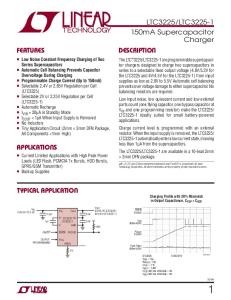
Typical Application
R0
D1
VB
VDD
VDD
VH
C0
IGBT Rg
C1
IN
IN
VSS
Datasheet
BF7610R2
HO
VS
WI-D06-J-0040 Rev.A/0
L
Page 1 of 8
BYD Microelectronics Co., Ltd.
BF7610R2
Pin Configuration ( Top View ) 1
VDD
VB
8
2
IN
HO
7
3
VS S
VS
6
4
NC
NC
5
Pin Definition Pin
Name
Description
1
VDD
Control Power Supply: connect 1µF capacitance to VSS for filtrating common-mode noise
2
IN
Control Signal Input: signal Input for High-side; High logic input is valid; pull-down to VSS by internal resistance
3
VSS
Ground
6
VS
Floating Supply Offset Voltage: up to 600V
7
HO
Driver Output
8
VB
Floating Power Supply: up to 620V
4, 5
NC
Not Connected
Block Diagram
VB
VDD
Pulse Filter
R
Q
HO
S
UV Detect
VS IN
Smitter
Filter
Pulse Gen
VSS
Datasheet
WI-D06-J-0040 Rev.A/0
Page 2 of 8
BYD Microelectronics Co., Ltd.
BF7610R2
Absolute Maximum Ratings Absolute maximum ratings indicate sustained limits beyond which damage to the device may occur. All voltage parameters are absolute voltages referenced to VSS unless otherwise specified. (TA=25°C) Definition
Min
Max
VDD
Control Power Supply
-0.3
20
VIN
Input Signal Voltage
-0.3
7
VB
High-side floating supply voltage
VS
VS +20
VS
High-side Floating Supply Offset Voltage
-0.3
600
VHO
Hide-side floating Output Voltage
VS-0.3
VB+0.3
Allowable Offset Supply Voltage Transient
-
50
TJ
Operating Junction Temperature (Note1)
-40
150
TS
Storage Temperature
-40
150
TL
Lead Temperature (soldering,10 seconds)
-
300
Symbol
dVS/dt
Units
V
V/ns
℃
Recommended Operating Condition All voltage parameters are absolute voltages referenced to VSS unless otherwise specified. (TA=25°C) Symbol
Parameter Definition
Min
Typ
Max
VDD
Control Supply Voltage
12
15
16.5
VB
High-Side Floating Supply Voltage
VS
VS +15
VS +20
Units
V -0.3
-
600
Logic Input Voltage
0
-
5
PWM Input Signal Frequency
-
-
20
kHz
Ambient Temperature
-20
-
125
℃
VS
High-side Floating Supply Offset Voltage
VIN fPWM TA
Datasheet
WI-D06-J-0040 Rev.A/0
Page 3 of 8
BYD Microelectronics Co., Ltd.
Electrical Characteristics
BF7610R2
( TA = 25°C, VDD=15V, unless otherwise noted )
Static Electrical Characteristics Symbol UVD
Parameter Definition VDD Under-voltage Protection
UVR
Conditions
Min.
Typ.
Max.
Detection voltage
8.8
10.1
11.2
Resetting voltage
9.8
11.1
12.2
VIN(ON)
Input ON Threshold Voltage
VDD=15V
3
-
-
VIN(OFF)
Input OFF Threshold Voltage
VDD=15V
-
-
0.8
IQDD
Quiescent VDD Supply Current
-
215
350
IQBS
Quiescent VBS Supply Current
-
20
80
ILK
Offset Supply Leakage Current
-
-
50
IIN+
Input Bias Current
VIN=3.3V
-
0.9
1.5
IIN-
Input Bias Current
VIN=0
-
0
-
IO+
Output High Short Circuit Pulsed Current
VO=0V, VIN=3.3V, PW≤10μs
170
250
-
IO-
Output low short circuit pulsed current
VO=15V, VIN=3.3V, PW≤10μs
360
510
-
VDD=15V,VIN=0, VDD-VSS VBS=15V, VIN=0, VB-VS VB=VS=600V
Units
V
µA
mA
Dynamic Electrical Characteristics Symbol ton tr toff
Parameter Definition
Min
Typ
Max
Turn-on Propagation Delay
-
400
550
Turn-on Rise Time
-
160
220
-
360
500
Turn-off Propagation Delay
Conditions
CL=1nF,VIN=03.3V (Figure 1)
tf
Turn-off Fall Time
-
75
120
TFILIN
Control Input Filter Time
100
160
-
Datasheet
WI-D06-J-0040 Rev.A/0
Units
Page 4 of 8
ns
BYD Microelectronics Co., Ltd.
BF7610R2
50%
50%
IN ton
toff
tr 90%
HO
tf
90%
10%
10%
Figure 1. Switching Times Definition
tfilin
tfilin
tfilin
tfilin
IN
HO
Figure 2. Input Noise Filter Function
Typical Performance Characteristics In Figure 3 ~ 6, VIN=03.3V, CL=1nF, TA = 25°C
Figure 3. Turn-on Time vs Supply Voltage
Datasheet
Figure 4. Turn-off Time vs Supply Voltage
WI-D06-J-0040 Rev.A/0
Page 5 of 8
BYD Microelectronics Co., Ltd.
BF7610R2
Figure 5. Turn-on Rise Time vs Supply Voltage
Figure 6. Turn-off Fall Time vs Supply Voltage
Applications Information Under-voltage protection ( Figure 7 ) b1: Normal operation b2: Under voltage detection (UVD) b3: Under voltage reset (UVR) b4: Normal operation
VDD
UVD
UVR
b2
b3
b4
b1
IN
HO Figure 7. Under-voltage Protection
Level shift capacitance and resistance Selection To calculate the capacitance value using the following formula: C0=IBS*T/ △V Where: T=max. turn on pulse width (logic „1‟ output) Datasheet
WI-D06-J-0040 Rev.A/0
Page 6 of 8
BYD Microelectronics Co., Ltd.
BF7610R2
IBS =IC drive current △ V = allowable discharge voltage. Considering credibility and dispersing specialty etc, commonly the choosing value is 2~3 times of calculating. The value of resistance R0 must ensure charge △ V back to C0 during the time C0*R0 and the minimal turn off pulse width. To calculate the resistance value using the following formula: R0= (| VDD – VBS | * t) / (C0 * △V) Where: VDD = Applied between VDD-VSS VBS = Applied between VB-VS t = min. turn off pulse width (logic „0‟ output)
Level shift diode Selection The voltage rating of the diode should meet the peak voltage rating of the converter (over 600V). Moreover, to achieve high efficiency a FWD is recommended. And the forward time is less than 100ns.
Package Description(Unit:Millimeter)
Symbol A A1 A2 B B1 C D E E1 e L E2 Min 3.710 0.510 3.200 0.380 0.204 9.000 6.200 7.320 3.000 8.400 1.524(BSC) 2.54(BSC) Max 4.310 3.600 0.570 0.360 9.400 6.600 7.920 3.600 9.000
Datasheet
WI-D06-J-0040 Rev.A/0
Page 7 of 8
BYD Microelectronics Co., Ltd.
BF7610R2
Restrictions On Product Use
The information contained herein is subject to change without notice.
BYD Microelectronics Co., Ltd. (short for BME) exerts the greatest possible effort to ensure high quality and reliability. Nevertheless, semiconductor devices in general can malfunction or fail due to their inherent electrical sensitivity and vulnerability to physical stress. It is the responsibility of the buyer, when utilizing BME products, to comply with the standards of safety in making a safe design for the entire system, including redundancy, fire-prevention measures, and malfunction prevention, to prevent any accidents, fires, or community damage that may ensue. In developing your designs, please ensure that BME products are used within specified operating ranges as set forth in the most recent BME products specifications.
The BME products listed in this document are intended for usage in general electronics applications (computer, personal equipment, office equipment, measuring equipment, industrial robotics, domestic appliances, etc.). These BME products are neither intended nor warranted for usage in equipment that requires extraordinarily high quality and/or reliability or a malfunction or failure of which may cause loss of human life or bodily injury (“Unintended Usage”). Unintended Usage include atomic energy control instruments, airplane or spaceship instruments, transportation instruments, traffic signal instruments, combustion control instruments, medical instruments, all types of safety devices, etc.. Unintended Usage of BME products listed in this document shall be made at the customer‟s own risk.
BME is not responsible for any problems caused by circuits or diagrams described herein whose related industrial properties, patents, or other rights belong to third parties. The application circuit examples explain typical applications of the products, and do not guarantee the success of any specific mass-production design.
Datasheet
WI-D06-J-0040
Rev.A/0
Page 8 of 8