International Research Journal of Engineering and Technology (IRJET)
e-ISSN: 2395-0056
Volume: 02 Issue: 05 | Aug-2015
p-ISSN: 2395-0072
www.irjet.net
A Low Noise Op-Amp Transimpedance Amplifier for InGaAs Photodetectors Bhaskar Mishra1, Dr. Kanika Sharma2, Pawan Choudhary3 1
M.E Scholar, Electronics & Communication Engineering, National Institute of Technical Teachers Training & Research, Chandigarh, India 2 Assistant Professor, Department of Electronics & Communication Engineering, National Institute of Technical Teachers Training & Research, Chandigarh, India 3 M.E Scholar, Electronics & Communication Engineering, National Institute of Technical Teachers Training & Research, Chandigarh, India
---------------------------------------------------------------------***---------------------------------------------------------------------
Abstract - The front-end design of the optical receiver contains a photodiode and transimpedance amplifier (TIA). It is a challenge to design an efficient transimpedance amplifier for optical receivers. TIA is used to convert low current signals ( ) into a proportional output voltage. Op-amp based TIA is used in several applications because the op-amps are an attractive option for the TIA gain element due to a range of wideband low noise devices are commercially available and likewise it is relatively easy to modify a design for particular requirements. In this paper, we purpose the modeling, the design, and the development of a low noise op-amp transimpedance amplifier for InGaAs photodetectors in order to record low level optical ) signals.
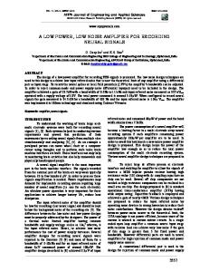
Key Words: Fiber Bragg Grating, Operational Amplifier, Photodiodes, and Transimpedance Amplifier. 1. INTRODUCTION Photodiodes and InGaAs Photodiode convert optical signals into current signal. These signals are usually small in magnitude (nA to μA in LIDAR applications [1], FBG sensor applications [2]) and are commonly amplified by a transimpedance amplifier (TIA) which converts the photocurrent into a proportional output voltage simultaneously amplifying the signal. It is also known as Ito-V converter [3]. An active transimpedance amplifier is based on active elements like BJTs, FETs, and operational amplifier (Opamp). Transimpedance amplifier using op-amp is the widely used one. Fig.1 shows the active op-amp based transimpedance amplifier circuit with photodiode. In the circuit shown in Fig.1, +V and –V are the supply voltages for the op-amp. and (necessary to maintain stability) are the feedback resistor and feedback capacitor respectively. is the photodiode current. The
Figure 1: Active op-amp based transimpedance amplifier with photodiode This paper describes the design, implementation and application of TIA based on the OPA656 wideband FET input op-amp.
1.1
Design Requirements
The design requirements for the TIA are: Transimpedance gain of at least 10000 V/A -3 dB bandwidth of at least 5 MHz. DC coupling of the photodiode to the TIA. Guaranteed stability with a photodiode capacitance of up to 10 pF.
2. DESIGN METHODOLOGY Methodology adopted in this paper includes selection of various performance parameters for the efficient designing for TIA and selection of suitable op-amp considering the performance parameters.
2.1 Selection of various performance parameters for the efficient designing of TIA Gain: The feedback resistor (
) value is used to
define the gain of the TIA. For gain to be very high, feedback resistor is made as large as other constraints permit. The value of the feedback resistor is [4]:
photodiode is connected between ground and the inverting input of the op-amp. The other input of the opamp is connected to ground. © 2015, IRJET
ISO 9001:2008 Certified Journal
Page 54
International Research Journal of Engineering and Technology (IRJET)
e-ISSN: 2395-0056
Volume: 02 Issue: 05 | Aug-2015
p-ISSN: 2395-0072
www.irjet.net
where
= maximum output voltage; = minimum output voltage:
capacitance of photodiode,
=
of the photodiode,
maximum input current of the photodiode. Bandwidth: The -3 dB bandwidth of the TIA is inversely proportional to the feedback resistor. Therefore, if the bandwidth is important then, small feedback resistor is used. Stability: To stabilize the transimpedance amplifier, a large enough capacitor must be placed in parallel with the feedback resistor. The calculated value of feedback capacitor is [5]:
where amp and
: Shunt resistance
: photodiode reverse light
current, and reverse bias voltage. Step 2: Calculate the total capacitance including the op-amp input capacitance photodiode capacitance
= total capacitance of the photodiode and
op-amp;
Step 1: Firstly examines and draw the equivalent circuit of the photodiode which contains the :
, and
.
Step 3: Determine the magnitude of the possible reverse light current output from the photodiode, including the minimum current anticipated and maximum current anticipated. Step 4: Choose a feedback resistor value such that the input current levels create the desired output signal voltages, and ensures that the output voltages can accommodate the dynamic range of the input signal. The value of the feedback resistor can be calculated by dividing the maximum output voltage by the maximum input current:
= gain-bandwidth product of the opis the feedback resistor.
Noise: It is essential to take into account various noise sources (internal and external). Internal noise sources within the op-amp and external noise which the TIA may pick up such as power supply noise.
Step 5: Calculate the optimum capacitance which is given as:
Step 6: Calculate the bandwidth given the resulting component values.
Step 7: Evaluate the circuit to determine if all design goals are satisfied and also conduct different types of simulations to determine the different properties of the circuit.
feedback
2.2 Selection of suitable op-amp considering the performance parameters First, calculate the required op-amp gain-bandwidth product, i.e. [4]
Also Op-amp with JFET or CMOS inputs are the most commonly selected type because these op-amps typically have much lower bias current than those with BJT input devices. This results in reduced DC error voltages and lower noise due to reduced input current noise. The OPA656 IC (Texas Instruments), is selected for this design because of its excellent combination of low bias current, offset voltage, power consumption and wide bandwidth.
3. SIMULATION The implementation of TIA coupled with the photodiode characteristics using NI Multisim Software. It includes the following steps: © 2015, IRJET
3.1 Simulation Types We will conduct three different types of simulations to determine the different properties of our TIA. First, we make an AC analysis to determine the frequency response and gain. The result of the AC analysis is displayed in two parts: gain versus frequency and phase versus frequency. Next we perform the transient analysis, after satisfying ourselves with the AC analysis. In transient analysis, also called time-domain transient analysis, Multisim computes the circuit’s response as a function of time. The result of the transient analysis is a calculation of voltage versus time. The last one is noise analysis. It performs an AC analysis to determine the noise. Noise analysis produces an output noise spectrum, an input noise spectrum and, optionally, a component contribution spectrum. When the
ISO 9001:2008 Certified Journal
Page 55
International Research Journal of Engineering and Technology (IRJET)
e-ISSN: 2395-0056
Volume: 02 Issue: 05 | Aug-2015
p-ISSN: 2395-0072
www.irjet.net
analysis is finished, its results are displayed as a graph of voltage squared, versus frequency, Hz [6, 7].
3.2 Transimpedance Amplifier with OPA656 in Multisim We have implemented the circuit shown in Figure 2 and have used the following values as our baseline values for simulations i.e., photodiode parameters.
(a)
(b) Figure 3: AC analysis (a) gain v/s frequency and (b) phase v/s frequency
Figure 2: Transimpedance amplifier, with OPA656 drawn in Multisim; Reverse light current I_S= 10 μA and the feedback resistance R_F=100kΩ
4.2 Transient Analysis
A high gain is first selected and the calculated (Equation
1)
is
.
capacitance is
Further,
the
photodiode
and the op-amp input
capacitances are
and
.
Total capacitance is the sum of photodiode and op-amp capacitance. Therefore . Using the formula for
(Equation 2) gives
value for
. This measured
gives too much ringing effect in the frequency
As we have decided on OPA656 as our preferred op-amp for TIA, we look closely at some of the circuit characteristics. We use the transient analysis to see how the circuit reacts to a specified input signal, and to observe the shape of our output signal. In Figure 4, we can see a typical input response of the transient analysis with OPA656. Our input signal for this analysis is a current signal which has a peak-to-peak value of 20 μA with a frequency of 1 kHz.
response curve. Some overcompensation can be used to reduce the ringing. So, the value for is finally considered to be
.
4. RESULTS AND DISCUSSION 4.1 AC Analysis (Gain and Bandwidth) The simulation results are shown in Figure 3. The top graph shows the gain of the TIA in decibels as a function of frequency of the input signal. The -3 dB bandwidth and the gain at -3 dB point are calculated to be 9.61 MHz and 97.02 dB respectively. The bottom graph shows the phase shift as a function of frequency. At -3 dB point, the phase drops to only 117 degrees from 180 degrees and the circuit remains stable. © 2015, IRJET
Figure 4: Input signal from transient analysis with OPA656 Figure 5 shows the output response of the transient analysis with OPA656. Our output signal for this analysis is a voltage signal which has a peak-to-peak value of 2V with a frequency of 1 kHz. As we are using an inverted
ISO 9001:2008 Certified Journal
Page 56
International Research Journal of Engineering and Technology (IRJET)
e-ISSN: 2395-0056
Volume: 02 Issue: 05 | Aug-2015
p-ISSN: 2395-0072
configuration, we see that
and
www.irjet.net
are inverted, as
REFERENCES
expected.
Figure 5: Output signal from transient analysis with OPA656
4.3 Noise Analysis Now, we perform the simulation in Multisim, to view the noise traces, as follows in Figure 6. The Figure 6 shows that the noise voltage is constant for lower frequencies. For higher frequencies the input noise voltage increases, the output noise voltage drops considerably with frequency increasing.
Figure 6: Noise power spectral density curves
5. Conclusion
[1] Akeel Auckloo, Richard Tozer, John David and Chee Hing Tan, "A low noise op-amp transimpedance amplifier for LIDAR applications”, proceedings of 21st IEEE International Conference on Electronics Circuits and Systems (ICECS), pp. 590-593, 2014. [2] T. Komljenovic, M. Bosiljevac, Z. Sipus, “Cost effective FBG based optical sensor”, 19th International Conference on Applied Electromagnetics and Communications, IEEE, pp.1-4, 2007. [3] R. A. Gayakwad, “Op-Amps and Linear Integrated Circuits”, Prentice Hall India, 1993. [4] M. Pachchigar, “Design Considerations for a Transimpedance Amplifier”, National Semiconductor Corporation, Application Note- 1803, 2008. http://www.ti.com/general/docs/lit/getliterature.ts p?literatureNumber=snoa515a&fileType=pdf. [5] John Caldwell, “1 MHz, single supply, photodiode amplifier reference design”, National Semiconductor Corporation, Application Note- tidu535, 2014. http://www.ti.com.cn/general/cn/docs/lit/getliterat ure.tsp?baseLiteratureNumber=tidu535&fileType=p df [6] Guo-hong, Yan, Zhang Shui-ying, and Du Jing-jing, “Practice and application of Multisim in digital electronic experiment teaching”, in 6th International Conference on Computer Science & Education (ICCSE), pp. 492-494, 2011. [7] Wang, Xiu-Ling, Jia-Ying Zhang, Wen-Lan Wang and Xiao-Dong Zhang, "Noise analysis for electronic circuit using Multisim”, in the 2nd IEEE International Conference on Information Management and Engineering (ICIME), pp. 324-326, 2010.
We have designed and simulated a low noise op-amp transimpedance amplifier for InGaAs photodetectors. We have simulated TIA circuit with NI Multisim (12.0.1) software. With low noise transimpedance amplifier, a bandwidth of ~ 9.61 MHz and a gain of ~99.99 kΩ have been achieved.
ACKNOWLEDGEMENT The authors would like to thank Dr. Bhargab Das, Scientist, CSIR-CSIO, Chandigarh, for his valuable advice in this work.
© 2015, IRJET
ISO 9001:2008 Certified Journal
Page 57
International Research Journal of Engineering and Technology (IRJET)
e-ISSN: 2395-0056
Volume: 02 Issue: 05 | Aug-2015
p-ISSN: 2395-0072
www.irjet.net
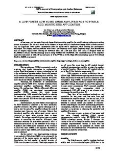
BIOGRAPHIES
s Photo
oto
Author’s P hoto
© 2015, IRJET
Bhaskar Mishra is currently enrolled at the Master’s programme (Electronics and Communication Engineering) at NITTTR, affiliated to Panjab University, Chandigarh. He received the B.E. degree in ECE from Rajasthan University, Jaipur, Rajasthan in 2009. Dr. Kanika Sharma received the Master of Engineering degree in Electronics & Communication from PEC, Panjab University, Chandigarh and her PhD in Electronics & Communication from Punjab Technical University, Chandigarh. She is currently employed as Assistant Professor at NITTTR, Chandigarh. Her research involves Embedded Systems, Digital System Designing, Wireless Sensor Networks, and Mobile Communication.
Pawan Choudhary is currently enrolled at the Master’s programme (Electronics and Communication Engineering) at NITTTR, affiliated to Panjab University, Chandigarh. He received the B.E. degree in ECE from Rajasthan University, Jaipur, Rajasthan in 2010.
ISO 9001:2008 Certified Journal
Page 58