A low noise, low power dynamic amplifier with common mode detect and a low power, low noise comparator for pipelined SAR-ADC by Santosh Prabhu Astgimath Supervisor: Prof. Dr. J.R. Long, TU Delft Dr. Klaas Bult, Broadcom Dr. F.M.L. Van Der Goes, Broadcom A thesis submitted in partial fulfillment for the degree of Master of Science in the Electronics Research Laboratory Faculty of Electrical Engineering, Mathematics and Computer Science DELFT UNIVERSITY OF TECHNOLOGY
August 2012
i
Thesis committee
Prof. Dr. John Long
Dr. Klaas Bult
Dr. Frank van der Goes
Dr. R. Bogdan Staszewski
Dr. Bert-Jan Kooij
Declaration of Authorship I, Santosh Prabhu Astgimath, declare that this thesis titled, ”A low noise, low power dynamic amplifier with common mode detect and a low power, low noise comparator for pipelined SAR-ADC” and the work presented in it is my own. I confirm that:
�
This work was done wholly while in candidature for a master’s degree at this University.
�
I have clearly attributed the work of others, which was consulted while doing this thesis. With the exception of such attributes, this thesis is entirely my own work.
�
I have acknowledged all main sources of help.
�
Copying or publishing this thesis for financial gain is not allowed without further written permission from Broadcom and that any user may be liable for copyright infringement.
�
This thesis can be made freely available for research purposes only after the disclosure stamp have been put on this document by Broadcom.
Signed: Santosh Prabhu Astgimath
Date: August 27, 2012
ii
DELFT UNIVERSITY OF TECHNOLOGY
Abstract Faculty of Electrical Engineering, Mathematics and Computer Science Electronics Research Laboratory Master of Science by Santosh Prabhu Astgimath
This thesis presents a high gain, low noise and low power dynamic residue amplifier and a low power, low noise dynamic comparator designed in TSMC 28nm process for a two step Pipelined SAR-ADC.
The cascoded integrator dynamic residue amplifier (CIDRA) achieves a gain of 30dB with THD of 47dB (11 mV pp input). The input referred noise across temperature and process corner is 55 µV and it operates at a frequency of 500MHz while the energy consumption is 390 fJ. The low power and low noise pseudo-latch preamp dynamic comparator (PLPDC) shows a delay of 250pSec for a differential input of 16 pV and consumes 91 fJ (current is 91 µA for 100 MHz clock) of energy. The input referred offset is 4 mV (σ).
Acknowledgements I came to TUDelft with an intention to learn new trends and to get different perspective about micro electronic design. Through this dissertation with confidence I can say that I have successfully met those objectives. The reason for my confidence are the people who taught me, guided me and supported me. And I would like to acknowledge these people who helped me during my entire masters project.
First and foremost, I would like to thank my supervisor, Dr. Klaas Bult for providing me this wonderful opportunity to work at Broadcom amongst an outstanding group of engineers. His knowledge and experience in analog design was a source of inspiration for me to take up challenging project out of my comfort zone. This internship would not have been possible without him. Detailed discussions with him are responsible for most of my learnings in this project. It was really a pleasure and honour to work under his guidance.
I would like to thank my promoter, Prof. Dr. John Long for providing the support and valuable feedback on my thesis, and taking care of all the administrative tasks involved in doing a masters thesis. I sincerely appreciate the patience he has shown, while correcting mistakes in my thesis.
I would also like extend my special thanks to Dr. Frank van der Goes for the mentor-ship and encouragement. In spite of his busy schedule Frank was always enthusiastic for discussions. Those interesting discussions have immensely helped me to understand the system, solve the circuit level issues and make circuits compatible to the system.
I learnt from my supervisors, that the presentation of the idea is as important as the idea by itself. Their valuable feedbacks on my thesis have helped me present the circuits in a simple but in a effective manner.
I would like to thank all the engineers at Broadcom Bunnik, in particular Chris iv
v Ward, Stefano Bozzola, Sijia Wang, Erol Arslan, Rohan Sehgal, Davide Vecchi, Jan Mulder, Jan Westra and Xiaodong Liu for numerous technical discussions and advices. And I consider myself very fortunate to have access to best of the best analog/RF design engineers. Els was always there for helping me out with all the administrative tasks, Thanks for being there.
The courses that I took during the first year of my masters were very inspirational, as they have shown me different approaches of thinking about analog design. Those courses have motivated me to think different. I would like to thank all the professors for those courses.
Leaving my family and coming to Delft was one of the hardest decision I made. It would be hard to put contributions of my parents (Prabhu and Sunanda) and my wife (Seema) in couple of lines. In simple words “My parents are the living gods”. And my wife has been the source of my strength which helped me go through tough times. Without their sacrifices, support, confidence, love and care this would never have happened. I am very thankful to my uncles (Basu kakar and Patted mamar), aunts (Nirmala aunty and Leela aunty) and Radhika for being there with my parents in my absence.
During the second year of my masters, I stayed with Th. M. Matton and J.W.MattonVermeulen. They have been very helpful and understanding, just like I would imagine my grand parents. I am very thankful to them for everything.
Finally I would like to thank all of my friends in India and Netherlands for all the support and encouragement. I have had very good memories with my friends which I will cherish for rest of my life.
Contents Declaration of Authorship
ii
Abstract
iii
Acknowledgements
iv
List of Figures
viii
List of Tables
xi
1 Introduction 1.1 ADC survey . . . . . . . . . . . . . . . . . . . . . . . . . . . . . . . 1.2 Specifications of the residue amplifier and comparators . . . . . . . 1.3 Organization of this thesis . . . . . . . . . . . . . . . . . . . . . . . 2 Overview of SAR-ADC and pipelined SAR-ADC 2.1 ADC performance metrics . . . . . . . . . . . . . . 2.2 SAR-ADC . . . . . . . . . . . . . . . . . . . . . . . 2.3 Pipelined SAR-ADC . . . . . . . . . . . . . . . . . 2.4 Derivation of specifications for residue amplifier and 2.5 Summary . . . . . . . . . . . . . . . . . . . . . . .
. . . . . . . . . . . . . . . . . . . . . comparator . . . . . . .
. . . . .
3 Noise bandwidth of a discrete time amplifier 3.1 Step response of a transconductance amplifier . . . . . . . . . . . 3.2 Gain and noise of the transconductance amplifier in the steady-state and integration modes of operation . . . . . . . . . . . . . . . . . 3.3 Comparison of steady state mode and integrator mode . . . . . . 3.4 Summary . . . . . . . . . . . . . . . . . . . . . . . . . . . . . . .
1 2 4 5
6 . 6 . 9 . 10 . 11 . 14 15 . 15 . 17 . 20 . 23
4 Dynamic residue amplifier 24 4.1 Gain of the dynamic amplifier circuits . . . . . . . . . . . . . . . . . 24 4.1.1 Single-stage integrator . . . . . . . . . . . . . . . . . . . . . 25 4.1.2 Cascoded integrator . . . . . . . . . . . . . . . . . . . . . . 27 vi
Contents 4.2 4.3 4.4 4.5
4.6
vii
Noise of the single-stage integrator and the cascoded integrator . . Comparison between single-stage integrator and cascoded integrator using simulations . . . . . . . . . . . . . . . . . . . . . . . . . Linearity of the cascoded integrator . . . . . . . . . . . . . . . . . Dynamic residue amplifier with cascoded integrator and commonmode detect . . . . . . . . . . . . . . . . . . . . . . . . . . . . . . 4.5.1 Common-mode detect . . . . . . . . . . . . . . . . . . . . 4.5.2 Design methodology for CIDRA . . . . . . . . . . . . . . . 4.5.3 Design parameters of CIDRA . . . . . . . . . . . . . . . . Summary . . . . . . . . . . . . . . . . . . . . . . . . . . . . . . .
5 Dynamic Comparator 5.1 Comparator circuits . . . . . . . . . . 5.1.1 Sense amplifier . . . . . . . . 5.1.2 Double-tail comparator . . . . 5.1.3 Pseudo-latch preamp dynamic 5.2 Design methodology for the PLPDC 5.3 Summary . . . . . . . . . . . . . . .
. . . . . . . . . . . . . . . . . . . . . . . . . . . . . . . . . . . . . . . comparator (PLPDC) . . . . . . . . . . . . . . . . . . . . . . . . . .
6 Calibration and configuration 6.1 Gain calibration for the CIDRA . . . . . . . 6.2 Integration time configuration for CIDRA . 6.3 Flicker noise reduction in CIDRA . . . . . . 6.4 Offset cancellation for PLPDC and CIDRA . 6.5 Summary . . . . . . . . . . . . . . . . . . .
. . . . .
. . . . .
. . . . .
. . . . .
. . . . .
. . . . .
. . . . .
. . . . .
. . . . .
. . . . . .
. . . . .
. . . . . .
. . . . .
. . . . . .
. . . . .
. 31 . 35 . 37 . . . . .
38 39 43 44 45
. . . . . .
47 47 48 49 50 57 61
. . . . .
62 62 63 65 66 67
7 Conclusions 68 7.1 Contributions . . . . . . . . . . . . . . . . . . . . . . . . . . . . . . 68 7.2 Summary . . . . . . . . . . . . . . . . . . . . . . . . . . . . . . . . 69 7.3 Limitations and suggestions for future work . . . . . . . . . . . . . 71
A Temperature and process corner simulation plots 73 A.1 Simulations of the CIDRA . . . . . . . . . . . . . . . . . . . . . . . 73 A.2 Simulations of the PLPDC . . . . . . . . . . . . . . . . . . . . . . . 78 B Layout and post layout simulations C Appendix C C.1 Gain of the differential single-stage integrator . . . . . . . . C.2 The noise and energy consumption of sense amplifier based parator . . . . . . . . . . . . . . . . . . . . . . . . . . . . . . C.3 Steady-state settling period and accuracy . . . . . . . . . . .
84 90 . . . . 90 com. . . . 91 . . . . 92
List of Figures 1.1 1.2 2.1 2.2 2.3 2.4 3.1
3.2 3.3 3.4 3.5 4.1 4.2 4.3 4.4 4.5 4.6 4.7
Figure of merit (FoM) verses Nyquist frequency (fsnyq) of recently published ADCs with SNDR≥55 [2] . . . . . . . . . . . . . . . . . Block diagram of pipelined SAR-ADC . . . . . . . . . . . . . . . . (a)SAR loop (b)5 cycles of SAR Loop with binary DAC . . . . . 14-bit pipelined SAR architecture . . . . . . . . . . . . . . . . . . Comparator/residue amplifier noise requirement for SAR-ADC and pipelined SAR-ADC . . . . . . . . . . . . . . . . . . . . . . . . . Over-range to correct the error from first stage of the pipelined SAR-ADC . . . . . . . . . . . . . . . . . . . . . . . . . . . . . . . Step response of transconductance amplifier (a) Transconductance amplifier with time constant τo (b)steady-state mode response (c) integrator mode response . . . . . . . . . . . . . . . . . . . . . . . Transconductance amplifier model (t ≤ 0 switch is closed; t > 0 switch is open) . . . . . . . . . . . . . . . . . . . . . . . . . . . . Step response of transconductance amplifier versus time for different time constant Ro values (τo = Ro C) . . . . . . . . . . . . . . . . . Step response of transconductance amplifier in the integrator mode versus time for different GCm values . . . . . . . . . . . . . . . . . . Gain, output referred noise and input referred noise versus τo . . .
2 3
. 9 . 10 . 11 . 12
. 16 . 17 . 20 . 22 . 23
(a) Single-stage integrator (b) Equivalent small signal model of single-stage integrator . . . . . . . . . . . . . . . . . . . . . . . . . 25 Graphical explanation of single-stage integrator functionality . . . . 26 Cascoded integrator . . . . . . . . . . . . . . . . . . . . . . . . . . . 28 Small signal models of Figure 4.3 (a) for phase-2 (b) for phase-3 (c) for phase-4 . . . . . . . . . . . . . . . . . . . . . . . . . . . . . . . 29 Graphical explanation of cascoded integrator functionality (C1=C2=C) 30 Calculation of the period ∆t12n due to the noise . . . . . . . . . . . 33 (a)The input-referred noise, gain and energy consumption of the single-stage integrator. Capacitor (C1) is varied from 40 fF to 140 fF (b) The input-referred noise, gain and energy consumption of cascoded integrator. Ratio between C1 and C2 is varied while keeping (C1 + C2 ) constant (equal to 140 fF) . . . . . . . . . . . . . . . 36
viii
List of Figures 4.8
4.9 4.10 4.11 4.12 4.13 4.14 4.15
ix
Simulation of linearity of the cascoded integrator with two-tone (50 MHz and 51 MHz) input with 11 mV pk-pk (see Table 4.1 for other parameters) (a) THD and gain versus sampling instance (ptstop) (b) Differential outputs versus time . . . . . . . . . . . . . . . . . . Simulation of the cascoded integrator of Figure 4.3 (see Table 4.1 for parameters) . . . . . . . . . . . . . . . . . . . . . . . . . . . . . The concept for common-mode detect circuit . . . . . . . . . . . . . Cascoded integrator dynamic residue amplifier (CIDRA) . . . . . . The transient simulation of CIDRA (a) One transient cycle (b) the CIDRA circuit (see Table 4.1 for parameters) . . . . . . . . . . . . A symmetric common-mode detect circuit with source degeneration The input-referred noise, gain, energy and integration time as a function of C1 (pcap ph1), where C1+C2=constant. . �. . . . . . . . scale down Input-referred noise and gain versus the aspect ratio W L factor (pctemp) for input pair and tail transistor. . . . . . . . . . .
37 38 40 40 41 42 43 44
5.1 5.2 5.3 5.4
Sense amplifier based comparator . . . . . . . . . . . . . . . . . . . 48 Double-tail comparator (a) Stage-1 (b) Stage-2 . . . . . . . . . . . . 50 Pseudo-latch preamp dynamic comparator . . . . . . . . . . . . . . 52 A transient decision cycle of the PLPDC of Figure 5.3 (a) individual node voltages (b) differential voltages . . . . . . . . . . . . . . . . . 53 5.5 Comparator delay measurement . . . . . . . . . . . . . . . . . . . . 55 5.6 All the three comparators designed with similar transistor sizes (comp1=Sense amplifier; comp8=Double-tail comparator; comp13=PLPDC) (a) Delay vs differential input voltage (pdvin) (b) Energy consumed vs differential input voltage (pdvin) . . . . . . . . . . . . . . . . . . 56 5.7 The input-referred noise , energy and delay as function of C1 and C2. The variable pctemp is the scale up factor for C1 and C2. . . . 57 5.8 Input-referred noise, gain, energy and time delay as a function of C1 (pcap ph1), where C1+C2=constant. . . . �. . . . . . . . . . . . 58 5.9 Input-referred noise versus the aspect ratio W scale down factor L (pctemp) for input pair and tail transistor. . . . . . . . . . . . . �. . 59 5.10 Input-referred noise and time delay versus the aspect ratio W L scale up factor (pctemp) for input pair and tail transistor. . . . . . 60 6.1 6.2 6.3 6.4 6.5 6.6
Input pair and cascode pair of CIDRA . . . . . . . . Gain versus V tpmic (pgccoarse in the picture) across temperature corner . . . . . . . . . . . . . . . . . . . Tail current source for integration time configuration Integration time Vs tail current (150 times pibias) . . Switch for flicker noise reduction . . . . . . . . . . . . Offset cancellation for PLPDC . . . . . . . . . . . . .
. . . . . . . process and . . . . . . . . . . . . . . . . . . . . . . . . . . . . . . . . . . .
. 63 . . . . .
64 64 65 66 66
A.1 CIDRA : Temperature and Corner simulations results of Gain and Energy/cycle . . . . . . . . . . . . . . . . . . . . . . . . . . . . . . 75
List of Figures A.2 CIDRA : Temperature and Corner simulations results of Noise(input referred) and Integration time . . . . . . . . . . . . . . . . . . . . . A.3 CIDRA : Temperature and Corner (two tone) simulation results of THD and IM3 . . . . . . . . . . . . . . . . . . . . . . . . . . . . . . A.4 CIDRA : Input referred offset before correction . . . . . . . . . . . A.5 CIDRA : Input referred offset after correction . . . . . . . . . . . . A.6 Comparator-1 : Temperature and Corner simulations results of Noise(input referred) and Energy/cycle . . . . . . . . . . . . . . . . A.7 Comparator-1 : Temperature and Corner simulations results of Delay) and Energy/cycle in the reset phase . . . . . . . . . . . . . . . A.8 Comparator-2 : Temperature and Corner simulations results of Noise(input referred) and Energy/cycle . . . . . . . . . . . . . . . . A.9 Comparator-2 : Temperature and Corner simulations results of Delay) and Energy/cycle in the reset phase . . . . . . . . . . . . . . . A.10 Comparator-1 : Input referred offset before correction . . . . . . . . A.11 Comparator-1 : Input referred offset after correction . . . . . . . . . A.12 Comparator-1 : voltage at gate of parallel input pair to cancel offset A.13 Comparator-2 : Input referred offset before correction . . . . . . . . A.14 Comparator-2 : Input referred offset after correction . . . . . . . . . A.15 Comparator-2 : voltage at gate of parallel input pair to cancel offset
x
75 76 77 77 79 79 80 80 81 81 82 82 83 83
B.1 CIDRA : Layout, and the size (width,hight) of this module is (85µm,41µm) 85 B.2 PLPDC-1: Layout, and the size (width,hight) of this module is (12µm,11µm) . . . . . . . . . . . . . . . . . . . . . . . . . . . . . . 86 B.3 PLPDC-2: Layout, and the size (width,hight) of this module is (12µm,11µm) . . . . . . . . . . . . . . . . . . . . . . . . . . . . . . 86 B.4 CIDRA : Differential voltage at drain of input pair and differential output of schematic and post layout simulations . . . . . . . . . . . 88 B.5 PLPDC-1 : Differential output voltage of schematic and post layout simulations . . . . . . . . . . . . . . . . . . . . . . . . . . . . . . . 88 B.6 PLPDC-2 : Differential output voltage of schematic and post layout simulations . . . . . . . . . . . . . . . . . . . . . . . . . . . . . . . 89 C.1 The input referred noise and the energy consumption of a sense amplifier based comparator . . . . . . . . . . . . . . . . . . . . . . . 92 C.2 Step response of the transconductance amplifier and accuracy(bits) versus normalized settling time . . . . . . . . . . . . . . . . . . . . 93
List of Tables 1.1 1.2 1.3 1.4 1.5
Sample specifications of the ADC lane . . . . . . . . . . ADCs which have achieved low figure of merit (FoM) [2] Primary specifications of the residue amplifier . . . . . . Primary specifications of the stage 1 comparator . . . . . Primary specifications of the stage 2 comparator . . . . .
2.1 2.2 2.3
Residue amplifier specifications († option for calibration) . . . . . . . 13 Stage1 comparator specifications . . . . . . . . . . . . . . . . . . . . 14 Stage2 comparator specifications . . . . . . . . . . . . . . . . . . . . 14
4.1 4.2
Parameters used for simulations of schematic shown in Figure 4.3 THD comparison for different common-mode detect methods (Input=11mV pk-pk, 50MHz and 51MHz) . . . . . . . . . . . . . . . Design parameters of CIDRA in Figure 4.11 . . . . . . . . . . . . Design parameters of common-mode detect shown in Figure 4.13 .
4.3 4.4 5.1
. . . . .
. . . . .
. . . . .
. . . . .
. . . . .
. . . . .
1 3 4 4 4
. 35 . 42 . 45 . 45
5.4 5.5 5.6 5.7
Advantages and disadvantages of the sense amplifier and the doubletail comparators . . . . . . . . . . . . . . . . . . . . . . . . . . . . . Parameters of sense amplifier comparator (see Figure 5.1) used for comparison . . . . . . . . . . . . . . . . . . . . . . . . . . . . . . . Parameters of double-tail comparator (see Figure 5.2) used for comparison . . . . . . . . . . . . . . . . . . . . . . . . . . . . . . . . . . Parameters of the PLPDC (see Figure 5.3) used for comparison . . Comparator comparison († error probability for 250ps operation time) Final parameters of the PLPDC for stage-1 (see Figure 5.3) . . . . Final parameters of the PLPDC for stage-2 (see Figure 5.3) . . . .
6.1
Process corners used for simulations . . . . . . . . . . . . . . . . . . 62
7.1 7.2
Specification compliance matrix for residue amplifier Stage1 comparator specification compliance matrix († correction) . . . . . . . . . . . . . . . . . . . . . . . . Stage2 comparator specification compliance matrix († correction) . . . . . . . . . . . . . . . . . . . . . . . .
5.2 5.3
7.3
51 54 54 55 56 59 60
. . . . . . . . 71 offset before . . . . . . . . 71 offset before . . . . . . . . 72
A.1 CIDRA : Initial drain voltage of input pair (pgccoarse) and tail current (pibias) calibration values . . . . . . . . . . . . . . . . . . . 74 xi
List of Tables
xii
B.1 CIDRA : Comparison between schematic and post layout simulations 87 B.2 PLPDC-1 : Comparison between schematic and post layout simulations . . . . . . . . . . . . . . . . . . . . . . . . . . . . . . . . . . 87 B.3 PLPDC-2 : Comparison between schematic and post layout simulations . . . . . . . . . . . . . . . . . . . . . . . . . . . . . . . . . . 87 C.1 Parameters of the figure 5.1 used for estimation of energy consumption 92
x
Chapter 1 Introduction The analog to digital converter (ADC) is one of the key components in communication systems. The low-power operation of ADCs help to reduce heat dissipation, thus allowing the use of low-cost packages. Low-power operation also increases battery life in hand-held communication devices. In such a communication system, the sampling rate needs to be in the range of giga-samples per second (greater than 1GS/s [1]). Time-interleaved ADC which has multiple ADC lanes operating in parallel, can meet high speed requirements. The input is sampled by each ADC lane successively separated by an equal time interval. It implies that each ADC lane can sample at a lower frequency (hundreds of MHz) than the overall ADC sampling frequency (giga-hertz). Based on internal research, Broadcom proposed the specification for a single ADC lane as given in Table 1.1. Table 1.1: Sample specifications of the ADC lane
Parameter
Specification
Units
Supply
1
Volts
Sampling clock
100
MHz
Peak-peak input signal
1.4
Volts
Reference voltage
0.7
Volts
ENOB
12
bits
Power
1
mW
1
Chapter 1. Introduction
2
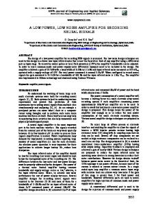
Figure 1.1: Figure of merit (FoM) verses Nyquist frequency (fsnyq) of recently published ADCs with SNDR≥55 [2]
1.1
ADC survey
As the required effective number of bits of the targeted ADC is 12, recently published ADCs with SNDR greater than 55dB were filtered from [2]. From the filtered list, low-power ADCs were considered for the implementation (eventually Broadcom intends to reach a figure of merit of 1fJ/conversion). Figure 1.1 shows figure of merit (FoM) vs Nyquist frequency (fsnyq) of recently published ADCs with an SNDR≥55dB. Some of the ADCs with a low FoM are also listed in Table 1.2 (highlighted with circles in Figure 1.1). It turns out that ADC types with a low FoM are mostly successive approximation (SAR) or pipelined SAR-ADCs. Hence, both SAR and pipelined SAR-ADCs were considered for the study, but to meet the desired specifications of the ADC shown in Table 1.1, a pipelined SAR-ADC is considered for implementation. The reasoning behind the selection is explained in Chapter 2. In this design the pipelined SAR-ADC has two stages, and each stage is a SARADC with a residue amplifier between them (see Figure 1.2). Apart from meeting noise and gain specifications, the residue amplifier should consume low energy (for this design, 400fJ). The concept of dynamic amplification has been used in the past
Chapter 1. Introduction
3
Table 1.2: ADCs which have achieved low figure of merit (FoM) [2]
First author
ADC type
Sampling rate
1 Harpe
SAR
4MS/s
2 Liu
SAR
SNDR (dB)
FoM (fJ/conversion)
Year of publication
58.3
6.5
2012
100MS/s
56
11.6
2010
3 Verbruggen Pipelined SAR
250MS/s
56
13.2
2012
4 Liu
SAR
100MS/s
60.29
21.9
2010
5 Walker
SAR
31.3kS/s
60.3
41.5
2011
6 Lee
Pipelined SAR
50MS/s
64.37
51.8
2010
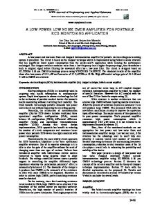
Figure 1.2: Block diagram of pipelined SAR-ADC
[3–5] for ADC designs. These ADCs consume power in the range of few mili-watts (1.4mW, 2.6mW and 1.7mW respectively). Hence, dynamic circuits have been chosen as a category of circuits for the study (more reasoning is provided in Chapter 3 and 4). In this dissertation, a low-noise, low-power cascoded-integrator dynamic residue amplifier (CIDRA) and a low-power, low-noise pseudo-latch preamp dynamic comparator (PLPDC) are designed for a pipelined SAR-ADC, to meet the proposed specification of Table 1.1.
Chapter 1. Introduction
1.2
4
Specifications of the residue amplifier and comparators
Let us assume that the ADC will be designed such that effective number of bits (ENOB) of the ADC is limited by thermal noise. The primary specifications for both amplifier and comparators are the input referred noise and the energy consumption. Considering an overall ENOB of 12 bits and 1mW power consumption, the budget for the input referred noise power and the energy consumption for the residue amplifier is shown in Table 1.3. Design of the residue amplifier with these specifications is the primary objective of this dissertation. Tables 1.4 and 1.5 show the input referred noise and energy consumption of the comparators for stage 1 and stage 2 respectively. The derivation of specifications for the sub-modules is presented in Chapter 2. Table 1.3: Primary specifications of the residue amplifier
Parameter
Typical
Units
Gain
16
V/V
Noise @ input
50
µVolts
Energy/cycle
400
fJ
Settling period
1
nsec
Table 1.4: Primary specifications of the stage 1 comparator
Parameter
Typical
Units
Noise @ input
300
µVolts
Energy/cycle
100
fJ
Delay (LSB input)
250
psec
Table 1.5: Primary specifications of the stage 2 comparator
Parameter
Typical
Units
Noise @ input
450
µVolts
Delay (LSB input)
150
psec
Chapter 1. Introduction
1.3
5
Organization of this thesis
Chapter 2 gives brief overview of SAR and pipelined SAR-ADC architectures. Chapter 3 describes the operating modes of the transconductance amplifier along with a mathematical analysis of the noise and gain of this amplifier. Chapter 4 presents a detailed analysis of basic dynamic structures for voltage amplification using the integration principle. Chapter 4 also presents the dynamic amplifier and its design methodology. Chapter 5 gives a brief survey of dynamic comparators and presents a pseudo-latch based dynamic comparator and its design methodology. The configuration and calibration options for the dynamic amplifier and dynamic comparator are discussed in Chapter 6. Chapter 7 concludes this dissertation with specification compliance matrices.
Chapter 2 Overview of SAR-ADC and pipelined SAR-ADC This chapter begins with definitions of ADC performance metrics. The subsequent section gives an introduction of the SAR-ADCs and its operation. The noise and energy requirements of the comparator for each cycle of the SAR-ADC are also analysed in section 2. Section three explains how a pipelined SAR architectures can reduce the energy consumption compared to just a SAR-ADC. The ADC concepts presented in this chapter is the result of a literature survey of recently published papers and discussion with my supervisors, they are not original ideas. These concepts are described to provide the motivation for the design of an amplifier and comparator. Specifications for the amplifier and comparators are derived in the final section.
2.1
ADC performance metrics
Differential non-linearity (DNL) is defined as the deviation of the step size in a non-ideal data converter from the ideal. If Xk is the transition point between
6
Chapter 2. Overview of SAR-ADC and pipelined SAR-ADC
7
successive codes k-1 and k, then the DNL of the ADC can be expressed as DN L(k) = ((Xk+1 –Xk ) − LSB)/LSB,
(2.1)
where least significant bit (LSB) is the ideal step size for that particular ADC [6].
Integral non-linearity (INL) is defined as the deviation of the actual transfer function from the straight line passing through the mid-points of the ideal input-output characteristic. The INL can be expressed as k X IN L(k) = DN L(l).
(2.2)
l=0
However, usually it is measured as the deviation with respect to a best-fit line. The use of best-fit line corrects for any gain and offset errors, which are acceptable in many applications, and gives more information about harmonic distortion [6].
Total Harmonic Distortion (THD) is defined as the ratio of the root-mean-square (RMS) sum of all harmonic components to the RMS value of the fundamental in a certain frequency band. In decibels, s T HD = 20 log
j P
A2 (kfin )
i=2
A(fin )
,
(2.3)
where A(kf in) is the amplitude of the harmonic tone present at the k-th multiple of input frequency, f in.
Third-order intermodulation distortion (IM3) appears for multi-tone input signal, as the non-linearity of the ADC causes mixing of the spectral components, generating tones at the sum and the difference of integer multiples of the input frequencies. For example, if the two input tones are at frequencies f1 and f2, then due to non-linearity of the ADC the two tones gets mixed. Two of the dominant
Chapter 2. Overview of SAR-ADC and pipelined SAR-ADC
8
spectral components (assuming a symmetric, differential design) that result due to this mixing will be of frequencies (2f1-f2) and (2f2-f1). The IM3 is calculated as the ratio of the RMS sum of these two tones to RMS value of the fundamental (f1 and f2) [6].
Signal-to-noise and distortion ratio (SNDR) is the ratio of the power of the fundamental to the total noise and distortion power within a certain frequency band, and can be written as, � SN DR = 10 log
signal power total noise and distortion power
� dB.
(2.4)
The SNDR depends on both the amplitude and the frequency of the signal. At low input levels, SNDR is limited by noise, while distortion dominates for higher signal levels.
Effective number of bits (ENOB) [8] of an ADC is a measure determined from the SNDR, − 1.76 . EN OB = SN DR 6.02
(2.5)
Figure of Merit (FoM) is a simple metric used to measure the energy efficiency of an ADC. While a number of FoMs have been proposed, the most popular one [7] takes into account the power consumption, signal bandwidth and the effective resolution of the ADC in the following way, F oM =
Power Consumption , 2EN OB .min{2BW, fs }
(2.6)
where BW is bandwidth and fs is the sampling frequency.
The comparator has limited time to settle. The metastability occurs when the output of the comparator reaches a voltage that is not detected by the following logic. The metastable condition introduces errors in the system. The error probability (P(e)) [6] of comparator can be estimated in terms of the least significant
Chapter 2. Overview of SAR-ADC and pipelined SAR-ADC
9
Figure 2.1: (a)SAR loop (b)5 cycles of SAR Loop with binary DAC
bit (VLSB ) and the minimum voltage (Vmin ) the comparator can detect (without metastable condition) as, P (e) =
Vmin . VLSB
(2.7)
The error probability of comparator should be several order lower than the system bit error rate (BER).
2.2
SAR-ADC
Figure 2.1(a) shows the block diagram of the typical successive approximation loop, and Figure 2.1(b) shows 5 SAR cycles with an N-bit binary digital to analog converter (DAC) and a comparator in the negative feedback SAR loop [8]. For � � V a binary DAC, the SAR cycle starts with the initial DAC voltage at ref , and 2 � � V decreases by ref during the next cycle. The DAC voltage changes by one-half 4 of the previous DAC voltage every cycle. Negative feedback in the SAR loop ensures that the DAC voltage moves such that the error between the input and the DAC voltage is reduced as directed by the comparator decision. At the end of N � � V SAR cycles, the error will be 2ref . N
For a SAR-ADC with a binary DAC, every cycle needs to converge to
Vref . 2N
If
the comparator makes an error (due to offset or noise), there is no mechanism
Chapter 2. Overview of SAR-ADC and pipelined SAR-ADC
10
to correct the code and all the SAR-ADC cycles must be low noise (decided by ENOB of the ADC) events.
2.3
Pipelined SAR-ADC
Figure 2.2 shows a 14 bit pipelined SAR architecture.
Two SAR-ADCs are
pipelined with a residue amplifier (DRA) in between.
Figure 2.2: 14-bit pipelined SAR architecture
If the second stage has over-range (refer to [6] for over-range and digital error correction), based on the second stage digital code errors introduced by comparator (due to offset or noise) are digitally corrected. Depending on the over-range the noise specification of the first stage comparator can be relaxed. The second stage of the pipeline receives an amplified residue as input. Based on the gain of the residue amplifier the noise requirements of subsequent pipelined stages are relaxed. Hence, residue amplification is the only one low noise event compared to single SAR-ADC (see figure 2.3). Because of these advantages, the pipelined SAR-ADC as proposed in [5, 9, 10] is becoming one of the popular choices for a low power ADC. The noise from the residue amplifier must be low enough (similar to the comparator noise specification in a SAR-ADC), and power consumption is
Chapter 2. Overview of SAR-ADC and pipelined SAR-ADC
11
comparable to a comparator in a binary SAR-ADC. The exact noise specifications are derived in the next section.
Figure 2.3: Comparator/residue amplifier noise requirement for SAR-ADC and pipelined SAR-ADC
2.4
Derivation of specifications for residue amplifier and comparator
Table 1.1 gives the ADC lane specifications. To meet these ADC specifications, a two-stage pipelined SAR-ADC architecture is chosen. The resolution of Pipelined SAR-ADC is limited by thermal noise (residue amplifier, DAC and comparator), distortion (residue amplifier and DAC) and the quantization noise. The ADC will be designed such that its resolution (ENOB=12bits) is limited by thermal noise. The ADC is designed for 14 bits so that the quantization noise does not limit ENOB.
Having a high residue amplifier gain relaxes the noise requirements of the second stage. The residue amplifier chosen for implementation is open loop (refer to Chapter 4), and the input swing is limited. Hence, at least seven bits need to be resolved in the first pipelined stage such that the residue is small enough for the amplifier to be linear. Rest of the 7 bits are resolved in the second pipelined stage
Chapter 2. Overview of SAR-ADC and pipelined SAR-ADC
12
with an additional bit for over-range [6].
The reference voltage for the ADC is ±0.7V (see Table 1.1). For ENOB of 12, the total noise budget for the ADC is
1.4√ 212 × 12
' 100uV [8]. To meet the total noise
specification, the input referred noise budget for the residue amplifier is 50uV. Since the second pipelined stage needs to resolve 7 bits, from equation (2.5) the THD of the residue amplifier should be greater than (7 + 1) × 6.02 + 1.76 ' 50dB. The comparator in the second stage is designed for input referred noise of 450uV. With a residue amplifier gain of 16 (i.e., 24 ), the total input referred noise due to q �2 = 57uV , which is still amplifier and second stage comparator is 50u2 + 450u 16 within the total noise budget.
Figure 2.4: Over-range to correct the error from first stage of the pipelined SAR-ADC
Considering that the first stage resolves 7 bits, the residue for the second stage would be
1.4 27
= 10.9375mV . The over-range [6] is budgeted to be ±5.46875mV
(see Figure 2.4). If the stage-1 SAR makes an error then the residue would fall in to over-range, this error can be digitally corrected (refer [6] for over-range and error correction). After offset correction the comparator (first stage) offset is budgeted to be less than ±1mV. Also, the 3σ input referred noise of the comparator is budgeted for 1mV, which makes input referred noise of the comparator less than 333uV. The errors due to the comparator of the first stage can be digitally corrected. The rest of the over-range is left for switching noise at the input of the
Chapter 2. Overview of SAR-ADC and pipelined SAR-ADC
13
comparator. As explained before the noise budget for second stage comparator is 450uV.
During one ADC conversion, the comparator and the DAC of the stage-1 SAR switch seven times, and the comparator and the DAC of the stage-2 SAR switch eight times. The energy/cycle budget for stage-1 comparator is 100fJ (the energy/conversion will be 700 fJ), and for stage-2 comparator energy/cycle will be slightly less as it has more relaxed noise specification. The residue amplifier operates only once in the entire conversion cycle and the energy budget is 400 fJ/cycle (refer to section C.2 in Appendix C).
The clock frequency for the ADC is 100 MHz. Both stage-1 SAR and stage-2 SAR have 5 nsec each for the conversion. In stage-1, 1 nsec is allocated for residue amplifier operation and 4 nsec is budgeted for 7 comparator cycles. In stage-2 all of the 5 nsec is budgeted for 8 comparator cycles.
Based on the above discussions the proposed specifications of the residue amplifier are shown in table 2.1. Specifications of stage-1 comparator and stage-2 comparator are given in Table 2.2 and Table 2.3 respectively.
Table 2.1: Residue amplifier specifications († option for calibration)
Parameter
Min
Typ Max
Units
Supply
1
Volts
Input common mode
0.6
Volts
1
nsec
Settling period
†
Differential Input Gain
11
†
Noise @ input THD Energy/cycle
22
mVolts
16
V/V
50
µVolts
50
dB 400
fJ
Chapter 2. Overview of SAR-ADC and pipelined SAR-ADC
14
Table 2.2: Stage1 comparator specifications
Parameter
Min
Typ Max
Units
Supply
1
Volts
Input common mode
0.6
Volts
Delay (LSB input)
250
psec
Noise @ input
300
µVolts
Energy/cycle
100
fJ
Table 2.3: Stage2 comparator specifications
Parameter
Min
Units
Supply
1
Volts
Input common mode
0.6
Volts
Delay (LSB input)
150
psec
Noise @ input
2.5
Typ Max
450
µVolts
Summary
In this chapter, the SAR-ADC architecture has been introduced. Noise and energy requirements of the comparator were presented. Splitting the SAR-ADC into two stages with a gain stage in between, reduces the noise requirements of comparator. That leads to the Pipelined SAR-ADC. The impact of the residue amplifier specifications on the specifications of pipelined SAR-ADC were briefly analysed. A high gain, low-power and low-noise residue amplifier is critical for reduction of overall power consumption. Finally to quantify the problem definition, the amplifier and the comparator specifications were derived.
Chapter 3 Noise bandwidth of a discrete time amplifier This chapter describes two operating cases (steady-state mode and integrator mode) of a transconductance amplifier based upon the output noise behaviour. Noise and gain of the two modes are analysed and compared using an example, and conclusions are presented. Since the application is an ADC, analysis is restricted to the discrete-time mode.
3.1
Step response of a transconductance amplifier
Let us consider an amplifier with low-pass (considering a resistor and a capacitor) transfer function and time constant of τo (see Figure 3.1a). For a DC step input; Figure 3.1b shows the response of the transconductance amplifier when Ts >> τo , and Figure 3.1c shows the response of the transconductance amplifier when Ts > τo (henceforth referred to as the steady-state mode), the output noise power is not a function of time. For the condition Ts 0 switch is open)
A unit step input is assumed for this analysis. The output voltage of the transconductance amplifier (shown in the Figure 3.2) can be expressed as, � � t Vo (t) = Vi (t) (Gm Ro ) 1 − e− τo .
(3.1)
The output voltage across the capacitor is a function of the time. Mathematically, two cases of operation can be derived. For the steady-state mode t >> τo , and t τo1 (refer section 3.2) where τo1 = Ro1 C. Let us consider a case where the required accuracy is N bits, where N is greater than 3. For N greater than 3 bit accuracy the settling time should be Ts = nτo1 where n > 2 (refer to section C.3 in AppendixC). The gain of the transconductance amplifier
Chapter 3. Noise bandwidth of a discrete time amplifier
21
in the steady-state mode is given by, GainSS = (Gm Ro1 ),
(3.11)
and the noise bandwidth (from equation (3.9)) is given by, � N BWSS =
1 4Ro1 C
For the integrator mode, the condition is Ts
Ro1 ). The integration period is still the same (Ts ). The period Ts can be substituted with nτo1 for the purpose of comparison between the two modes. The gain of the transconductance amplifier in the integrator mode is given by, � GainIM =
Gm Ts C
� = nGm Ro1 ,
⇒ GainIM = nGainSS , where n > 2.
(3.13) (3.14)
Noise bandwidth of the transconductance amplifier in the integrator mode is given by, �
� � �� � 1 2 1 N BWIM = = . 2Ts n 4Ro1 C � � 2 ⇒ N BWIM = N BWSS , where n > 2. n
(3.15) (3.16)
From equations (3.14) and (3.16) the following conclusions can be drawn. For a fixed amplification time, the integrator mode shows less input-referred noise compared to steady-state mode due to the smaller noise bandwidth. For a fixed amplification time, the integrator mode achieves a higher gain than the steadystate mode. Figure 3.4 shows step response of transconductance amplifier in the integrator mode for different
Gm C
values. As long as transconductance (Gm ) and
integration period (TS ) is constant the input referred noise will not change even
Chapter 3. Noise bandwidth of a discrete time amplifier
22
though the slopes are different. Hence, slope can be adjusted to get the similar gain as that of steady-state mode. However, in the integrator mode the output is a function of time and it does not settle during Ts . Hence, to use the integrator mode for voltage amplification, it is essential that the integration time is well controlled to ensure final accuracy.
Figure 3.4: Step response of transconductance amplifier in the integrator mode versus time for different GCm values
To confirm the above analysis, large-signal simulation was done using the model in Figure 3.2 with transient noise (a feature available in Cadence Spectre). The simulation is done for fixed sampling time of 1 nsec and transconductance is 1 mS. The time constant τ has been varied from 0.1 nsec to 100 nsec (by varying resistor Ro ). Figure 3.5 shows the simulation results. The input-referred noise for the integrator mode is less than that for steady-state mode.
It will be seen in the next chapter that dynamic amplifiers inherently operate in the integrator mode. Hence, dynamic circuits were chosen for study and the design of the residue amplifier.
Chapter 3. Noise bandwidth of a discrete time amplifier
23
Figure 3.5: Gain, output referred noise and input referred noise versus τo
3.4
Summary
Based on the output noise behaviour, two modes of operation of transconductance amplifier were discussed in this chapter. The two modes were compared in terms of gain and noise. With a mathematical analysis using the non-stationary noise model of the transconductance amplifier, it was shown for a given clock frequency that the integrator mode is more beneficial in terms of noise. This analysis was supported by simulation results. Due to low noise, the residue amplifier topology operating in the integrator mode is considered for the residue amplification in Chapter 4.
Chapter 4 Dynamic residue amplifier This chapter presents a detailed analysis of a single-stage integrator and a cascoded integrator, and compares them in terms of gain and noise. As it was discussed in Chapter 3, the integrator output does not settle. Hence, to complete the topology of the dynamic amplifier a common-mode detect circuit is included to generate the stop signal, creating a cascoded integrator dynamic residue amplifier (CIDRA). The gain, noise and linearity of the CIDRA are then further analysed theoretically. Finally, simulation results are presented to support the analysis.
4.1
Gain of the dynamic amplifier circuits
The concept of dynamic amplifiers is not new as they have been a part of dynamic comparators as pre-amplifiers. Recently dynamic amplifiers have also been published [3–5, 13]. Typical characteristic of these dynamic amplifiers is that they do not need a constant DC bias current. The power consumption of dynamic amplifiers is proportional to clock frequency. As explained in Chapter 3, operating in the integrator mode is beneficial in terms of noise and gain. In the following sections two dynamic amplifier circuits are analysed for residue amplification in a pipelined ADC application, and both of them operate in the integrator mode.
24
Chapter 4. Dynamic residue amplifier
4.1.1
25
Single-stage integrator
A simple integrator can be built using one transistor pair (for differential operation). Figure 4.1 shows a simple (and intuitive) circuit of a dynamic amplifier.
Figure 4.1: (a) Single-stage integrator (b) Equivalent small signal model of single-stage integrator
The functionality of the single-stage integrator (used in [13]) is explained graphically in Figure 4.2. The operation can be explained in three phases. In the first phase, CLK is low. It is the reset phase for the amplifier. In this phase, the capacitors C1 are charged to avdd. The input pair is off. In the second phase, CLK is high. The tail of the input pair discharges to ground and hence the input pair turns ON. The input pair is in the saturation state. The differential nodes Vtm and Vtp discharge in proportion to the differential input (∆Vin = Vip − Vim ) through the input pair. Integration happens in this phase simultaneously the output common-mode moves towards the ground. The CLK is high in the third phase. The differential output signal builds on output capacitors C1. It continues to build until either Vtm or Vtp reach ground potential. In this phase, the input pairs are close to the linear region. The output signal should be stored at the end of the phase-2 when the transistors are still in saturation.
Chapter 4. Dynamic residue amplifier
26
Figure 4.2: Graphical explanation of single-stage integrator functionality
The expression for the gain for the single-stage integrator can be given by the following equation (refer to the section C.1 in Appendix C),
Ao =
Tint1 gm1 . 2C1
(4.1)
Where gm1 is the transconductance of each device in the input pair (assuming small ∆I). The integration time Tint1 can be expressed in terms of output common-mode voltage (Vocm ) as,
Tint1 =
Vocm C1 . Im
(4.2)
m2 In this expression Im is the output common mode current ( Im1 +I ) and can be 2
expressed as (assume basic MOS equation):
Chapter 4. Dynamic residue amplifier
gm1 =
27
2Im , Vgt
(4.3)
where Vgt is equal to Vgs − Vtn of the input pair. By substituting equations (4.2) and (4.3) into equation (4.1), the expression for the gain can be simplified as,
Ao =
Vocm . Vgt
(4.4)
As the differential output voltage (Vtp-Vtm) increases over time, the output common-mode voltage droops (see Figure 4.2). For a given output common-mode voltage and overdrive, the gain is fixed. For example, if the Vgt is 80mV (assuming that input pair is biased in weak inversion [14]) and the output common-mode voltage is 0.5V, the gain is 6.25. This limitation in gain comes because of limited supply voltages (1V in our design). The limitation in gain can be overcome by cascoding the integrator as explained in the next section.
4.1.2
Cascoded integrator
The optimization of a single-stage integrator is less flexible due to few design parameters. The cascoded integrator (see Figure 4.3) has two integrators connected in series. The gates of the cascode devices are shorted to node Vcb (a DC supply unless otherwise mentioned). Its functionality can be described in 5 phases. The 5 phases are also illustrated graphically in Figure 4.5. In phase-1 CLK is low. It is the reset phase for the amplifier. In this phase, both capacitors C1 and C2 are charged to avdd. The input pair (M1 and M2) and the cascode pair (M3 and M4) are cut-off. In the second phase, CLK is high (see Figure 4.4(a)). The source of the input pair discharges to ground and hence the input pair turns ON, and it is saturated. The cascode pair is still off. Nodes Vtm and Vtp discharge proportional to ∆Vin
Chapter 4. Dynamic residue amplifier
28
Figure 4.3: Cascoded integrator
through the input pair, while differential voltage ∆Vt = Vtm − Vtp increases over time. Integration happens in this phase (shown as Tint1 in Figure 4.5). In phase-3, CLK is high. When Vtm (or Vtp ) drops one Vt below Vcb , the corresponding cascode device turns on (see Figure 4.4(b)) and is in saturation. Approximately half of the common-mode current flows out of C2 connected at Vom (or Vop ). Now that the cascode device is on, it prevents Vtm (or Vtp ) from dropping further. Hence, ∆Vt starts dropping towards ground, and ∆t12 (only one cascode device is on) is proportional to the differential input voltage (see Figure 4.5). Hence, the differential voltage that is integrated at node Vom during ∆t12 is proportional to the input voltage. In phase-4, CLK is high. When the other node Vtp (or Vtm ) also drops Vt below Vcb , the second cascode device also turns ON, and is in saturation (see Figure 4.4(c)). The cascode pair prevents Vtp (or Vtm ) from dropping further. The differential output voltage continues to grow proportional to the differential input voltage but with a smaller slope compared to phase-3. The output common-mode voltage drops further.
Chapter 4. Dynamic residue amplifier
29
Figure 4.4: Small signal models of Figure 4.3 (a) for phase-2 (b) for phase-3 (c) for phase-4
In phase-5, CLK is still high. In this phase, both cascode devices enter the linear region. The beginning of phase-5 can be controlled by Vcb . Even though the output voltage continues to grow, the linearity of the transfer function degrades. Hence, it is essential that the differential voltage in phase-4 is stored, and that the circuit is prevented from entering in to phase-5. The output voltage across the cascoded integrator continues to integrate starting from the amplified voltage produced by the first stage, like two cascaded singlestage integrators. This is equivalent to increasing the supply voltage for a singlestage integrator. At the end of the tint1 + ∆t12 time period, the output voltage always follows the line
∆I C2
(see Figure 4.5). The gain at the end of the integration period Tint1 + Tint2
can be expressed as given below,
Ao =
gm1 (Tint1 + Tint2 ) . 2C2
(4.5)
Chapter 4. Dynamic residue amplifier
Figure 4.5:
30
Graphical explanation of cascoded integrator functionality (C1=C2=C)
Where gm1 (assuming that Im1 − Im2 is very small) is the transconductance of each device in the input pair. For very small input (∆Vin ), ∆t12 is very small compared to Tint1 + Tint2 . The integration periods Tint1 and Tint2 can be expressed in terms of output common-mode voltage drop (Vtn ) as given by following equations (for mathematical simplicity the common-mode voltage drop during Tint1 at the drain of the input pair is assumed to be the same as the output common-mode voltage drop during Tint2 ),
Tint1 =
Vtn C1 , Im
(4.6)
Tint2 =
Vtn C2 . Im
(4.7)
Chapter 4. Dynamic residue amplifier
31
Where Im is the common-mode current given by the equation,
gm1 =
2Im . Vgt
(4.8)
By substituting equations (4.6), (4.7) and (4.8) in to equation (4.5) the expression for the gain can be simplified as,
Vtn Ao = Vgt
�
C1 1+ C2
� (4.9)
By comparing equation (4.9) with equation (4.4) it is clear that cascoded integrator can achieve higher gain compared to the single-stage integrator by properly adjusting the ratio of C1 and C2 . This circuit operates in integrator mode, where output impedance of transistors does not influence the gain. Hence, cascoding alone does not increase the gain. The gain increases by cascoding, as long as C1 2 2 exists and C1 > C2 . However, the maximum gain can not be more than gm ro
(where gm and ro are transconductance and output impedance of transistors M1M4 respectively) [14].
4.2
Noise of the single-stage integrator and the cascoded integrator
From equation (3.10) of Chapter 3, the input-referred noise of the single-stage integrator at the end of the integration period (i.e., T int1 in Figure 4.2) can be expressed as,
2 VinoiseSI =
2kT 1 � . gm1 T int1 2
(4.10)
Chapter 4. Dynamic residue amplifier
32
By substituting Tint1 from equation (4.2) (and Im from equation (4.3)) into the equation (4.10), the input-referred noise of the single-stage integrator can be further simplified as,
2 VinoiseSI =
2kT Vgt . C1 Vocm
(4.11)
The factor 2 appears in the equation (4.11) because of the differential pair. Consider figures 4.3 and 4.5 for the noise analysis of cascoded integrator. The noise is modelled in phase4 (see Figure 4.5). The major contributor is the noise of the input pair. Since the cascode pair is degenerated by a MOSFET in saturation, it is assumed that the cascode pair does not contribute any noise. The noise from the input pair is present during the entire integration period, Tint1 + Tint2 . Currents Im1, Im2, Im3 and Im4 are assumed to be equal (i.e., Im ) for the rest of the noise analysis. The period ∆t12n used in the following equations highlights that it is ∆t12 due to noise. As explained previously, during Tint1 the cascode pair is off and noise (from the input pair) is integrated at the nodes Vtm and Vtp . During Tint2 the cascode pair turns on, and noise is integrated at the output nodes. To calculate the total output noise at the end of the period Tint1 + Tint2 , it is essential that noise during the period Tint1 is included in the analysis. The output referred noise for the cascoded integrator structure can be determined with the following approach. Assuming that the input voltage is zero the large signal behaviour of the circuit would still follow the graphical representation as shown in Figure 4.5. Noise can be found by mainly considering the behaviour in phase2 and phase4. Phase3 also exists, but the period ∆t12n is very small compared to Tint1 + Tint2 as it is only due to noise. For the mathematical analysis of the noise, calculating the period ∆t12n due to noise is essential. Hence, first the noise voltage (Vn1 ) at the end of the period Tint1 is calculated using equation (3.8b). Then the noise voltage (Vn1 ) is converted into the period ∆t12n using the common-mode slope of nodes Vtm and Vtp, which is
Im C1
(see Figure 4.6).
Chapter 4. Dynamic residue amplifier
33
Figure 4.6: Calculation of the period ∆t12n due to the noise
Considering that the cascode pair (M3 and M4) is off, the noise power at the nodes Vtp and Vtm during the phase2 can be written as (see the equation (3.8b)), 2 Vn1 =
2kT gm1 2 Tint1 . C12
(4.12)
The corresponding ∆t12n due to the input pair noise can be expressed as, ∆t212n
� =
C1 Im
�2
2 Vn1 .
(4.13)
During the period ∆t12n , the noise generated at the nodes Vtp or Vtm is transferred to output nodes Vop or Vom through one of the cascode transistors. Current Im flows through the cascode and C2. Hence, the noise power due to ∆t12n at the output is given by, 2 Vn12
=
∆t212n
�
Im C2
�2
� =
C1 C2
�2
2 Vn1 .
(4.14)
Assuming that the noise current flows only into C2 , the expression for the output noise power during Tint2 can be expressed as (refer to equation (3.8b)), 2 Vn2 =
2kT gm1 2 Tint2 . C22
(4.15)
2 2 Even though the noise powers Vn12 and Vn2 originate from the same source, they
are calculated at different time instances. Hence, the total output referred noise
Chapter 4. Dynamic residue amplifier
34
at the end of period Tint1 + Tint2 can be expressed as, 2 2 2 Vonoise = Vn12 + Vn2 .
(4.16)
By substituting the noise powers from phase2 (4.14) and phase4 (4.15) into equation (4.16), the output-referred noise can be written as, 2 Vonoise
� =
C1 C2
�2
2 + Vn1
kT gm1 Tint2 . C22
(4.17)
By substituting equation (4.12) into equation (4.17), the output referred noise can be further simplified as, 2 Vonoise =
kT gm1 (Tint1 + Tint2 ) . C22
(4.18)
The noise can be referred to the input of amplifier as given below, 2 Vinoise =
2 Vonoise . A2o
(4.19)
By substituting equation (4.5) into equation (4.19), the input-referred noise can be further expressed as, 2 Vinoise
� =
4kT gm1
�
1 . (Tint1 + Tint2 )
(4.20)
The equation (4.20) shows that, the input-referred noise still follows the basic integration principles of single-stage integrator (as explained in Chapter 3) even though the structure is cascoded. By substituting Tint1 and Tint2 from equations (4.6), (4.7) and (4.8) into equation (4.20), the input-referred noise of the cascoded integrator can be further simplified as,
2 Vinoise
� =
2kT C1 + C2
�
Vgt . Vtn
(4.21)
By comparing equation (4.21) with equation (4.11) it is clear that as long as the
Chapter 4. Dynamic residue amplifier
35
total capacitance is kept constant (and Vocm = Vtn ), the input-referred noise remains the same for both the single-stage and the cascoded integrators. However, the cascoded integrator can achieve a higher gain by redistributing the capacitors, without degrading noise or increasing the total capacitance. As long as the total capacitance is same, the energy consumption also remains the same.
4.3
Comparison between single-stage integrator and cascoded integrator using simulations
To verify the predictions from sections 4.1 and 4.2, large-signal simulations were done (with the circuit parameters given in Table 4.1) for the single-stage integrator (see Figure 4.1a) and the cascoded integrator (see Figure 4.3). The input pair (M1 and M2) of the single-stage integrator is same as that of the cascoded integrator. The simulation is done with a total capacitance of 140 fF.
Table 4.1: Parameters used for simulations of schematic shown in Figure 4.3
Parameter
Value
Input pair (M1 and M2)
40 ×
Cascode pair (M3 and M4)
20 ×
Tail switch (M5)
10 ×
1µ 0.06µ 1µ 0.06µ 1µ 0.03µ
C1
80 fF
C2
60 fF
Supply
1V
Input common-mode
0.5 V
The gain, noise and the energy consumption are compared between the singlestage integrator and the cascoded integrator (see Figure 4.7). Increasing the size of capacitor C1 for single-stage integrator reduces the noise because the integration period increases (integration period must be changed due to common-mode droop). For C1 equal to 140fF (integration period of around 330psec), the noise
Chapter 4. Dynamic residue amplifier
36
Figure 4.7: (a)The input-referred noise, gain and energy consumption of the single-stage integrator. Capacitor (C1) is varied from 40 fF to 140 fF (b) The input-referred noise, gain and energy consumption of cascoded integrator. Ratio between C1 and C2 is varied while keeping (C1 + C2 ) constant (equal to 140 fF)
of the single-stage integrator is 52uV. The redistribution of capacitance does not change the noise (between 56uV and 59uV) in the cascoded integrator. However, the redistribution of the capacitors helps to increase the gain. Since the total capacitance is same, the energy consumed by the cascoded integrator is almost similar to the single-stage integrator (' 200fJ). For a single-stage integrator, the gain for C1=40fF is smaller than for C1=60fF because of the leakage current.
For a cascoded integrator with a total capacitance of 140fF (assuming T = 300o K Vtn=0.5V and Vgt=0.08V) the expected input-referred noise is 97.3uV (see equation (4.21)). To be consistent with Chapter 3 the noise from MOSFET is considered as 4kT gm instead of 38 kT gm . The parasitic capacitors are neglected in the calculation. Hence, estimated noise is higher than the simulated noise (58uV). And for C1 = 80f F and C2 = 60f F the expected gain is 14.6 V/V (see equation (4.9)), and the simulated gain is 17.5 V/V.
Chapter 4. Dynamic residue amplifier
4.4
37
Linearity of the cascoded integrator
As analysed before, to ensure a linear transfer function for the amplifier, it is essential that the output voltage is stored before the devices enter the linear region at the end of phase4. To measure the linearity, a two-tone simulation was done for cascoded integrator (for circuit parameters see Table 4.1). Figure 4.8a shows the total harmonic distortion (THD) calculated from a two-tone simulation. The output was sampled at different points around the peak of the differential output (indicated by ptstop in Figure 4.8).
Figure 4.8: Simulation of linearity of the cascoded integrator with two-tone (50 MHz and 51 MHz) input with 11 mV pk-pk (see Table 4.1 for other parameters) (a) THD and gain versus sampling instance (ptstop) (b) Differential outputs versus time
As discussed in Chapter 2, resolving more bits in the second pipelined stage is more energy efficient. The higher the amplifier gain the smaller the energy consumption in the second stage, as higher noise can be tolerated from the second stage. Gains of up to 30 are possible with this circuit. However, the choice of gain also depends on linearity. For a fixed gain the linearity depends on the input voltage swing. A gain of 16 is assumed for design as it simplifies the digital post processing of two ADC outputs. To measure the linearity of the cascoded integrator, a two-tone (50MHz and 51MHz) simulation was performed (see Figure 4.8). If 7 bits are
Chapter 4. Dynamic residue amplifier
38
resolved in the first stage, then the residue is 11mV peak to peak. For an 11mV (peak to peak) input (each tone with 5.5mV pk-pk) with a gain of 16, the THD at the output is 65 dB (see Figure 4.8a), which is sufficient to resolve rest of the 8 bits in the second stage. The maximum linearity (65 dB) is limited by the linearity of the differential input pair. The non-linearity of the basic differential pair occurs because the drain current is proportional to the square of the Vgt of the input pair [14]. The THD when the gain peaks is poor, because the devices are in the linear region.
4.5
Dynamic residue amplifier with cascoded integrator and common-mode detect
Figure 4.9: Simulation of the cascoded integrator of Figure 4.3 (see Table 4.1 for parameters)
As seen in Figure 4.9 the differential output falls back to zero, and the differential output must be stored before the devices enter the linear region (see Figure 4.8). To store the differential output voltage the gate of the cascode devices (M3 and
Chapter 4. Dynamic residue amplifier
39
M4 in Figure 4.3) can be switched from Vcb to zero volts. Two approaches can be followed to generate this stop signal for the gate. First, an independent clock generator can be used. However, synchronization of clock with respect to amplifier (across process and temperature corner) and the jitter or the noise of such a clock generator must be considered in the design. The other approach is to generate the stop signal as a function of the output common-mode voltage. The noise of the output nodes is well controlled (designed for specified noise) and thus generated stop signal will be synchronous with the amplifier. Hence, following the second approach a common-mode detect circuit has been developed as described in the following section.
4.5.1
Common-mode detect
The output of the cascoded integrator (Vop and Vom in Figure 4.3) is input to the common-mode detect circuit. The output of common-mode detect circuit should � � om V op+V om be high if V op+V is above a threshold (' 0.5V). When falls below 2 2 the threshold, the output of the common-mode detect should be low.
Figure 4.10(a) shows the concept of common-mode detect circuit. For an NMOS input cascoded integrator, two parallel PMOS transistors would cancel the differential signal at the output and will be sensitive to the common-mode voltage alone. The current flowing in the PMOS transistors needs to be dropped across a load (see Figure 4.10(b)). Having a resistor as the load would consume DC current, hence a complementary (CMOS) topology is used. A NAND circuit is suitable (see Figure 4.10(c)). The output of NAND gate needs to be inverted and then connected to gate of the cascode. Thus, the overall operation of the common-mode detect is an AND.
Figure 4.11 shows the complete schematic of cascoded integrator dynamic residue amplifier (CIDRA). Turning off the cascode prevents C2 from discharging. Along
Chapter 4. Dynamic residue amplifier
40
with C2, if C1 is also stopped from discharging, more energy can be saved as the smaller the voltage change across the capacitor the smaller the energy consumption (Ctot V 2 , where Ctot = 2(C1 + C2 )). Hence, the clock for the tail switch has been gated (a simple digital AND gate) with Vcb , and the energy consumption of CIDRA is therefore significantly less than Ctot V 2 .
Figure 4.10: The concept for common-mode detect circuit
Figure 4.11: Cascoded integrator dynamic residue amplifier (CIDRA)
Figure 4.12 shows one transient cycle of the CIDRA. When the clock (phi1) goes high, nodes Vtp and Vtm start to integrate the input voltage. Outputs Vop and Vom are initially at the supply voltage as the cascodes are off. Hence, the output of the common-mode mode detect (Vcb) is high. When nodes Vtp and Vtm drop one Vt below the gate of the cascode pair, the cascode pair turns on
Chapter 4. Dynamic residue amplifier
41
and an amplified differential signal develops at outputs Vop and Vom. Meanwhile, � om the output common-mode voltage V op+V drops towards the ground. When 2 it crosses a threshold voltage (' 0.5 V) the output voltage common-mode detect (Vcb) becomes zero. The cascode pair turns OFF when the gate voltage (Vcb) drops to zero. With the cascode pair turned off, the amplified differential output voltage remains stored across the output capacitors, C2 .
Figure 4.12: The transient simulation of CIDRA (a) One transient cycle (b) the CIDRA circuit (see Table 4.1 for parameters)
With the common-mode detect circuit, the stop signal becomes a function of the output common-mode voltage of the amplifier. The most critical specification of the common-mode detect circuit is its sensitivity towards the signal. If the common-mode detect circuit is sensitive to differential-mode signal, the integration period would vary according to the signal level and hence the gain would be a function of the signal, causing distortion. To make the common-mode detect less sensitive to the differential signal, following two changes were included in the NAND circuit. Firstly, parallel PMOS transistors are degenerated by resistors (M7-M8, in Figure 4.13 transistors in the linear region), and secondly the NMOS load is made symmetric (M1-M4). The improved common-mode detect circuit is
Chapter 4. Dynamic residue amplifier
42
shown in Figure 4.13.
Figure 4.13: A symmetric common-mode detect circuit with source degeneration
Table 4.2 shows a comparison of THD (from two-tone simulations) for different conditions. The common-mode detect circuit is sized such that threshold is around 0.5 V. All of the methods have a same integration period and similar gain. From the table, it is clear that with a symmetric and degenerated common-mode detect circuit, the amplifier THD is 57dB, which is sufficient to resolve 8 bits in the second stage.
Table 4.2: THD comparison for different common-mode detect methods (Input=11mV pk-pk, 50MHz and 51MHz)
Common-mode detect method Ideal CMD
Gain
THD Before Sample THD after Sample
15
64dB
61dB
Simple AND gate
16.7
62dB
50dB
Symmetric and Degenerated AND gate
16.78
62dB
57dB
Chapter 4. Dynamic residue amplifier
4.5.2
43
Design methodology for CIDRA
The absence of DC bias current makes the design of dynamic structures unconventional. Even though the gain and noise depend on similar circuit parameters they can be optimized orthogonally. Given noise, gain and Ttot specifications, the following design methodology can be adopted for the design of CIDRA.
Figure 4.14: The input-referred noise, gain, energy and integration time as a function of C1 (pcap ph1), where C1+C2=constant.
As C1 increases, the total integration period Tint (see Figure 4.14 Tint = Tint1 + Tint2 ) increases. Hence, increasing C1 (while keeping C1 + C2 constant) reduces the noise. Increasing C1 increases the gain (see equation (4.21)). Even though the sum C1 + C2 is constant, energy increases with increasing C1 because the commonmode voltage swing is higher across C1 .
The minimum value of C2 is determined by the gate capacitance of the cascode. When Vcb switches from the supply to ground, the cascoded devices turn off and gate charge is injected into C2 . However, C2 is the stage-2 DAC capacitance in
Chapter 4. Dynamic residue amplifier
44
this design. Hence, for all practical purposes the minimum C2 is determined by the resolution of the second stage SAR.
Figure 4.15: Input-referred noise and gain versus the aspect ratio down factor (pctemp) for input pair and tail transistor.
W L
�
scale
The gain is inversely proportional to Vgt of the input pair (see equation (4.9)). Hence reducing Vgt of the input pair increases the gain. The input-referred noise is proportional Vgt (see equation (4.21)), hence, reducing Vgt of the input pair reduces noise. Both the input pair size and the tail transistor size (switch or active source) of CIDRA decides the Vgt of the input pair. Scaling down the input and tail (M1,M2 and M5 in Figure 4.11) transistors together keeps both the noise and gain constant while the parasitics are reduced (see Figure 4.15).
4.5.3
Design parameters of CIDRA
Based on the design methodology explained in the previous section the transistor and capacitor sizes are finalized. The minimum capacitor C2 for the second
Chapter 4. Dynamic residue amplifier
45
pipelined stage (SAR2) is 100 fF (considering DAC resolution in the second stage). Considering C2 and the parasitic capacitance due to common-mode detect circuit, the capacitor C1 has been scaled up such that the typical gain is around 20 (see equation (4.21)). Table 4.3 lists the final design parameters for the casoded integrator. Table 4.4 shows the design parameters of common-mode detect circuit. Corner simulations of this design are presented in Appendix A.
Table 4.3: Design parameters of CIDRA in Figure 4.11
Parameter
Value
Input pair (M1 and M2)
40 ×
Cascode pair (M3 and M4)
20 ×
Tail switch (M5)
10 ×
1µ 0.06µ 1µ 0.06µ 1µ 0.03µ
C1
400 fF
C2
100 fF
Supply
1V
Input common-mode
0.6 V
Table 4.4: Design parameters of common-mode detect shown in Figure 4.13
Parameter
Value
NMOS (M1 - M4)
0.12µ 1µ 4 × 0.36µ 0.03µ 20 × 0.12µ 0.08µ
PMOS (M5 and M6) Degenerating PMOS (M7 and M8)
4.6
Summary
Along with an introduction to dynamic amplifiers, two dynamic amplifier structures were discussed. Noise, energy consumption and gain were analysed in detail for both single-stage and cascoded integrators. The cascoded integrator shows an advantage in terms of gain. A common-mode detect circuit has been developed from a NAND gate circuit. Combining the integrator and common-mode detect
Chapter 4. Dynamic residue amplifier
46
circuits, a cascoded integrator dynamic residue amplifier (CIDRA) has been presented. For the given noise and gain specifications, a design methodology has been presented for the CIDRA to optimize its energy consumption and speed.
Chapter 5 Dynamic Comparator In the first section of this chapter, comparator circuits are discussed. In the subsequent section, a low power, low noise pseudo-latch preamp dynamic comparator (PLPDC) topology is presented. Three different comparators are compared in terms of noise, delay and energy consumption. The chapter concludes with a description of the design methodology and simulation results of the PLPDC.
5.1
Comparator circuits
Comparators are key modules for data converters as level detection is an important part of the overall operation. Minimizing the noise of the comparator is essential for high resolution ADCs. When compared to a SAR-ADC, the noise specifications of the comparators are relaxed in the pipelined SAR-ADC. The maximum noise allowed for the first stage comparator is limited by the over-range [6] in the second pipelined stage, and the maximum noise allowed for the second stage comparator is decided by the gain of the residue amplifier. In a SAR-ADC conversion cycle, the comparator and the DAC are the most active switching modules. Hence it is essential that comparator meets the noise and speed specification with the lowest power. Dynamic comparators do not need DC bias current, and they also follow
47
Chapter 5. Dynamic comparator
48
noise integration principles (refer to Chapter 3). Therefore, dynamic comparators are chosen for the study and the implementation.
5.1.1
Sense amplifier
Figure 5.1 shows one of the well-known latch-type sense amplifier circuits used in memories. Different variations of this circuit are present in the literature [15, 16]. The sense amplifier topology partially (M1-M4 and M7) resembles cascoded integrator (see Figure 4.3 in Chapter 4). In addition to cascoded integrator the sense amplifier has PMOS transistors (M5 and M6) and the outputs are cross coupled. The functionality of this comparator is explained in five phases (see Figure 5.1).
Figure 5.1: Sense amplifier based comparator
The first four phases of sense amplifier operation also resembles the cascoded integrator operation (see section 4.1.2 in Chapter 4). Till the forth phase the PMOS transistors remain cut-off, and the input signal is amplified by the cascoded integrator structure. Hence, first four phases can be considered as preamp part of the comparator operation.
Chapter 5. Dynamic comparator
49
The output noise power of this comparator is determined by the preamp phases of the operation. Since the preamp operation is similar to cascoded integrator operation, the integrator based noise analysis explained in section 4.2 of Chapter 4 is also applicable for this structure. As per the analysis, increasing the capacitance at nodes Vtm /Vtp and Vom /Vop increases the integration period and the noise reduces. The fifth phase begins when the output Vom (or Vop ) drops one PMOS threshold voltage below supply, the transistor M6 turns ON first and after a delay of (∆t12 ) other PMOS (M5) also turns ON. The latch comprising of two inverters (M3, M5, M4 and M6) becomes active. The pre-amplified signal at nodes Vop and Vom is further amplified by latch until the absolute differential output voltage reaches to supply. During the latch operation all the transistors (M1-M7) are ON, and there is a direct path from supply to ground. The longer the latch period, the more the current is leaked from supply to ground (especially with small differential input voltage). This direct current does not help in any way for the operation, hence, it should be reduced. For low noise, latch needs large transistors, and large transistors increase the parasitic capacitors. During the latch operation the voltage changes at the outputs (Vop/Vom) and (Vtp/Vtm) couple to the input of the comparator through the parasitic capacitors (Cgd of input pair) leading to unwanted kick-back noise.
5.1.2
Double-tail comparator
Figure 5.2 shows a two stage comparator [17] which is inspired by the double-tail comparator [18]. Due to two stages, the preamp and the latch can be optimized independently. The first stage (M1-M3 in the Figure 5.2a) of this circuit is a single-stage integrator (refer to section 4.1.1 in Chapter 4) and the second stage is cross-coupled latch (M4-M9 in Figure 5.2b). The gain of the single-stage integrator is less than the cascoded integrator gain. The lack of gain in the first stage makes
Chapter 5. Dynamic comparator
50
the noise produced by the second stage also significant in the total noise power at the output. Hence, this comparator circuit is noisier than the sense amplifier (see Table 5.5). However, since it has two-stages the kick-back noise from latch to the input will be smaller than the sense amplifier.
Figure 5.2: Double-tail comparator (a) Stage-1 (b) Stage-2
5.1.3
Pseudo-latch preamp dynamic comparator (PLPDC)
Table 5.1 summarises the advantages and disadvantages of the two comparators discussed previously. Having a cascoded integrator in the first stage is beneficial for low noise. To reduce direct current from supply to ground, the latch should be as small as possible and also fast. Increasing the gain of the pre-amplifier helps to reduce the input-referred noise due to the latch, thus allowing a reduction of the latch size. Considering these aspects, a two-stage pseudo-latch preamp dynamic comparator (PLPDC) (see Figure 5.3) has been derived. The preamp includes a cascoded integrator. Unlike the sense amplifier, the absence of PMOS transistors in the preamp avoids any direct current from the supply to ground. The cross-coupling of the NMOS cascodes increases the gain due to positive feedback. The cross-coupling in the preamp is done with only NMOS
Chapter 5. Dynamic comparator
51
Table 5.1: Advantages and disadvantages of the sense amplifier and the double-tail comparators
Comparator type
Advantage
Disadvantage
Sense amplifier
It has cascoded integrator as preamp (high gain structure), which is good for low input-referred noise
For low noise the latch needs large transistors. Large transistors in latch increase power consumption due to direct path from supply to ground
Double-tail
It has two stages, allowing independent optimization of the latch. Smaller kick back noise
It has single-stage integrator as preamp (small gain). Hence, noise due to second stage is also significant, thus input-referred noise is high.
and no PMOS, hence the name pseudo-latch preamp. Due to the large gain in the preamp (compared to the single stage integrator) the second stage (latch) can be small (compared to preamp) making the circuit power efficient. For better noise performance, the latch in the double-tail circuit needs M6 and M7 to be bigger, which adds parasitic capacitance. The transconductance of M6 and M7 in the double-tail is less compared to the sense amplifier because of degeneration. Because of the above two reasons, the second stage of the double-tail comparator is slow compared to the sense amplifier. Hence, the sense amplifier circuit (without tail transistor M7) is used as the second stage. Figure 5.4 shows one transient cycle of PLPDC, and the functionality is explained below in four phases. In the first phase CLK is low. It is the reset phase for the comparator, and all of the transistors are OFF. In the second phase, CLK is high. The source (Vtail in Figure 5.3a) of the input pair discharges to ground, and hence the input pair turns ON, and it is saturated. The differential nodes Vtm1 and Vtp1 discharge in proportion to ∆Vin through the input pair. Integration of the input signal at Vip and Vim happens in this phase. In the third phase, CLK is high. When Vtm1 (or Vtp1 ) drops one Vt below Vtp2 (or Vtm2 ), the corresponding cascode device M3 (see Figure 5.3a) turns on, and
Chapter 5. Dynamic comparator
52
Figure 5.3: Pseudo-latch preamp dynamic comparator
it is in saturation. Half of the common-mode current flows out of Vom (or Vop ). The period (∆t12 ) for which only one of the cascode (M3) is ON is proportional to the differential input voltage. Hence, the differential voltage that is integrated at node Vtm2 during that period (∆t12 ) is proportional to the input voltage. As Vtm2 (or Vtp2 ) starts dropping faster due to latch (M3 and M4) action, it slows down the discharging of the node Vtp2 (or Vtm2 ). The voltage difference between the nodes Vtp2 and Vtm2 would eventually reach the threshold of NMOS (due to the pseudo-latch). This is the preamp phase of the comparator, and it is similar to the cascoded integrator operation (see section 4.1.2 in Chapter 4). In the forth phase, CLK is high. When the output of preamp Vtm2 (or Vtp2 ) drops by one threshold voltage (of PMOS) below the supply, PMOS transistor M6 (see Figure 5.3b) turns on first. And after some delay the other PMOS transistor M7 also turns on. The cross-coupled latch (M8-M11) further amplifies the signal until the absolute differential output voltage reaches the supply. To verify the theoretical analysis, all three comparators were simulated. All three designs have similar transistor sizes in the first stage (see tables 5.2, 5.3 and 5.4).
Chapter 5. Dynamic comparator
53
Figure 5.4: A transient decision cycle of the PLPDC of Figure 5.3 (a) individual node voltages (b) differential voltages
The second stage latch is 30 times smaller than the preamp for both the doubletail comparator and the PLPDC. The second stage input pair (M6 and M7) for the double-tail is made slightly bigger than the PLPDC, because for the same size double-tail was showing very high input-referred noise. However, the size is increased, ensuring that total energy consumption of the double-tail is similar to the PLPDC.
Chapter 5. Dynamic comparator
54
Table 5.2: Parameters of sense amplifier comparator (see Figure 5.1) used for comparison
Parameter Input pair (M1 and M2)
Value 8×
NMOS Cascode pair (M3 and M4) 4 × PMOS pair (M5 and M6)
4×
Tail switch (M7)
4×
1µ 0.03µ 1µ 0.03µ 1µ 0.03µ 0.5µ 0.03µ
C1
3fF
C2
3fF
Supply
1V
Input common-mode
0.6V
Table 5.3: Parameters of double-tail comparator (see Figure 5.2) used for comparison
Parameter Input pair (M1 and M2) Tail switch (M3)
Value 4
2nd stage PMOS (M4 and M5) 2nd stage PMOS input pair (M6 and M7) 2nd stage NMOS (M8 and M9)
1µ 0.03µ 0.5µ × 0.03µ 0.24µ 0.03µ 1µ × 0.03µ 0.24µ 0.03µ
8×
2
C1
3fF
C2
3fF
Supply
1V
Input common-mode
0.6V
Chapter 5. Dynamic comparator
55
Table 5.4: Parameters of the PLPDC (see Figure 5.3) used for comparison
Parameter Input pair (M1 and M2)
Value
NMOS cascode pair (M3 and M4)
4
Tail switch (M5)
4
2nd stage PMOS input pair (M6 and M7) 2nd stage PMOS (M8 and M9) 2nd stage NMOS (M10 and M11)
1µ 0.03µ 1µ × 0.03µ 0.5µ × 0.03µ 0.5µ 0.03µ 0.24µ 0.03µ 0.24µ 0.03µ
8×
C1
3fF
C2
3fF
Supply
1V
Input common-mode
0.6V
Figure 5.5: Comparator delay measurement
The comparator delay is measured as shown in Figure 5.5, where vop and vom are the comparator outputs. Figure 5.6 shows the comparison between the three circuits in terms of time delay and energy consumption as a function of input voltage. The table 5.5 shows the comparison between three comparators. The following conclusions are specific to the simulation results for the parameters shown in tables 5.2, 5.3 and 5.4. Due to lack of the gain in the first stage, the double-tail comparator is slow and noisy (416 uV) compared to other two circuits. To meet the similar input referred noise as sense amplifier (151uV), the capacitors � 416u in double tail comparator needs to be increased by more than twice 151u = 2.75 ,
Chapter 5. Dynamic comparator
56
Figure 5.6: All the three comparators designed with similar transistor sizes (comp1=Sense amplifier; comp8=Double-tail comparator; comp13=PLPDC) (a) Delay vs differential input voltage (pdvin) (b) Energy consumed vs differential input voltage (pdvin)
and the energy consumption will also increase proportional to the capacitor. The large latch in the sense amplifier comparator leaks current during the latching phase and it is a function of input (see Figure 5.6). The PLPDC consumes slightly less energy compared to sense amplifier for similar input referred noise and delay (see Figure 5.6 and Table 5.5). Since comparator is switched several times during the SAR cycle (14 times), reduction in comparator power would be helpful. Since PLPDC is a two-stage circuit with a small latch, it will show less kick back noise compared to sense amplifier.
Table 5.5: Comparator comparison († error probability for 250ps operation time)
Comparator
Delay (1 µV input)
Energy (1 µV input)
Input noise
referred
Error probability †
Sense amplifier
140 psec
91 fJ
151 µV
10−9.23
Double-tail
310 psec
75 fJ
416 µV
10−0.73
PLPDC
150 psec
75 fJ
154 µV
10−8.13
Chapter 5. Dynamic comparator
5.2
57
Design methodology for the PLPDC
The design methodology of the PLPDC is similar to the CIDRA because both of them use a cascoded integrator. The following design methodology explains the optimization of speed and energy for a given noise specification for the comparator. Keeping the input pair in weak inversion ensures low noise. Increasing C1 and C2 together reduces noise, but it also increases the delay and energy consumption (see Figure 5.7).
Figure 5.7: The input-referred noise , energy and delay as function of C1 and C2. The variable pctemp is the scale up factor for C1 and C2.
As discussed previously for the cascoded integrator, increasing C1 for a fixed total capacitance of C1 + C2 gives higher gain in the preamp section. Hence, the noise remains constant but the speed improves (as illustrated by Figure 5.8).
Chapter 5. Dynamic comparator
58
Figure 5.8: Input-referred noise, gain, energy and time delay as a function of C1 (pcap ph1), where C1+C2=constant.
Once the noise specification is satisfied, scaling down the transistor sizes reduces the kickback noise and any additional energy loss. Figure 5.9 shows the effect of scaling down of the input pair and the tail transistor on the input-referred noise. If the input pair alone is scaled down, then the input-referred noise increases. However, if the tail switch is scaled down as well, Vgt of the input pair remains constant and hence the input-referred noise remains constant. On the other hand, if both the input pair and tail transistors are scaled up together, the speed of the circuit improves (see Figure 5.10), while the input-referred noise remains the same. Based on this design methodology the transistor and capacitor sizes are finalized. Tables 5.6 and 5.7 show the design parameters of the PLPDC for stage-1 and stage-2 SAR-ADCs, respectively. Corner simulations for these designs have been presented in Appendix A.
Chapter 5. Dynamic comparator
59
� Figure 5.9: Input-referred noise versus the aspect ratio W L scale down factor (pctemp) for input pair and tail transistor. Table 5.6: Final parameters of the PLPDC for stage-1 (see Figure 5.3)
Parameter Input pair (M1 and M2)
Value
NMOS cascode pair (M3 and M4)
6
Tail switch (M5)
4
2nd stage PMOS input pair (M6 and M7) 2nd stage PMOS (M8 and M9) 2nd stage NMOS (M10 and M11)
1µ 0.03µ 1µ × 0.03µ 0.5µ × 0.03µ 0.5µ 0.03µ 0.24µ 0.03µ 0.24µ 0.03µ
12 ×
C1
24 fF
C2
5.6 fF
Supply
1V
Input common-mode
0.6V
Chapter 5. Dynamic comparator
60
Figure 5.10: Input-referred noise and time delay versus the aspect ratio scale up factor (pctemp) for input pair and tail transistor.
W L
Table 5.7: Final parameters of the PLPDC for stage-2 (see Figure 5.3)
Parameter Input pair (M1 and M2)
Value
NMOS cascode pair (M3 and M4)
4
Tail switch (M5)
2
2nd stage PMOS input pair (M6 and M7) 2nd stage PMOS (M8 and M9) 2nd stage NMOS (M10 and M11)
1µ 0.03µ 1µ × 0.03µ 0.5µ × 0.03µ 0.5µ 0.03µ 0.24µ 0.03µ 0.24µ 0.03µ
8×
C1
6 fF
C2
2.8 fF
Supply
1V
Input common-mode
0.6 V
�
Chapter 5. Dynamic comparator
5.3
61
Summary
Three different comparator circuits were compared in this chapter. The pros and cons of each were discussed. For the design presented in Table 5.2, Table 5.3 and Table 5.4, the double tail comparator is noisy and slow compared PLPDC. For the similar noise performance the PLPDC consumes slightly less energy compared to sense amplifier. Finally, for a given noise specification, a design methodology has been presented for the PLPDC to optimize its speed and energy consumption.
Chapter 6 Calibration and configuration The cascoded integrator dynamic residue amplifier (CIDRA) and pseudo-latch preamp dynamic comparator (PLPDC) need additional calibration and configurations in order to have better control over gain, noise and offset. In this chapter, gain calibration and a configuration option for integration time for the CIDRA are discussed. The final section presents an offset cancellation setup for the PLPDC. The simulations are done for process corners (listed in Table 6.1) and also as the temperature is varied from −40o C to 125o C. Table 6.1: Process corners used for simulations
Name
Description
typicalmid.scs
Both NMOS and PMOS are in the typical corner.
fasthigh.scs
Both NMOS and PMOS are in the fast corner.
fnsphigh.scs
The NMOS is in the fast and the PMOS is in the slow corner.
snfphigh.scs
The NMOS is in the slow and the PMOS is in the fast corner.
slowhigh.scs
Both NMOS and PMOS are in the slow corner.
6.1
Gain calibration for the CIDRA
The CIDRA is an open-loop structure. The gain can be controlled by controlling the overall integration time. The integration period is determined by the initial 62
Chapter 6. Calibration and configuration
63
voltage(V tpmic ) at the drain of the input pair and the gate voltage of the cascode pair (Vcb) (see Figure 6.1). A more generic expression for the gain of CIDRA can be given as,
�
Aog
V tpmic − (V cb − Vtn ) = Vgt1
�� � C1 1+ . C2
(6.1)
If V tpmic = V cb, then equation (6.1) is same as that of equation (4.9). Although the typical maximum gain of that CIDRA is as high as 30, a gain of 16 (i.e., 24 ) is selected after considering linearity, process (see Table 6.1) and temperature variations. Figure 6.2 shows that with an appropriate initial condition at node V tpmic , a gain of 16 is achievable across all corners.
Figure 6.1: Input pair and cascode pair of CIDRA
6.2
Integration time configuration for CIDRA
For external noise sources like the DAC switches and reference, the CIDRA acts as a low-pass filter. The bandwidth of the CIDRA can be controlled by varying its integration time. This idea was suggested by Dr. F.M.L. Van Der Goes. Integration time, hence bandwidth can be controlled by varying the tail current (Itail ),
Chapter 6. Calibration and configuration
64
Figure 6.2: Gain versus V tpmic (pgccoarse in the picture) across process and temperature corner
so the tail switch is replaced by a current source (see Figure 6.3).
Figure 6.3: Tail current source for integration time configuration
The Vgt (overdrive) of input pair varies as the square root of the tail current. The gain should be calibrated to account for any changes due to variations in a tail current. To limit the external noise due to the DAC switches (effective resistance is 100 Ω) and the reference buffer (output impedance is 1kΩ), the integration time of 1nsec (refer to equation (3.10)) is required (see Figure 6.4) across all process
Chapter 6. Calibration and configuration
65
(see Table 6.1) and temperature corners. The actual tail current is scaled by 150 times the pibias using a current mirror.
Figure 6.4: Integration time Vs tail current (150 times pibias)
6.3
Flicker noise reduction in CIDRA
Due to the dynamic operation of the CIDRA, a simple technique has been used to reduce flicker noise. By frequently switching the input pair between strong inversion and accumulation the flicker noise can be reduced [19] (suggested by Dr. Klaas Bult). The interface traps can be flushed (hence reducing the flicker noise) by bringing the device into accumulation. An additional switch M6 is introduced at the source of the input pair (see Figure 6.5) to bias the transistors in the accumulation mode during the CIDRA inactive phase in order to reduce flicker noise.
Chapter 6. Calibration and configuration
66
Figure 6.5: Switch for flicker noise reduction
6.4
Offset cancellation for PLPDC and CIDRA
Offset of the PLPDC is cancelled by adding a parallel input pair (M1’ and M2’ in Figure 6.6). The gate voltage of the new input pair is varied to cancel the offset. This idea was suggested by Dr. F.M.L. Van Der Goes, and it is an existing technique used in Broadcom. Since this additional input pair leaks the charge from C1 without integration, the noise performance degrades. Hence, the area of offset cancelling pair M1’ and M2’ is scaled down by a factor of 6 compared to input pair M1 and M2 to reduce the charge leakage.
Figure 6.6: Offset cancellation for PLPDC
The offset of the CIDRA is cancelled by changing the DC reference voltage at the gate of the input pair. It can be implemented as part of the DAC. The offset of
Chapter 6. Calibration and configuration
67
the PLPDC can also be cancelled with a similar method (but it is not used in this implementation).
6.5
Summary
In this chapter, a gain calibration method and a technique to configure the integration time for the CIDRA was presented. A simple technique to reduce flicker noise by switching off the input pair was discussed. Finally, an offset cancellation method for the PLPDC was presented.
Chapter 7 Conclusions In this chapter, my contributions to this project are clearly described. In the second section, the thesis is summarized by comparing the simulated results with expected specifications for the amplifier and the comparator. In the final section, some design improvements are suggested.
7.1
Contributions
To build a low power and high resolution ADC, the SAR ADC and the pipelined SAR-ADC architectures as described in the chapter 2 were suggested by my supervisors in Broadcom, Dr. Klaas Bult and Dr. F.M.L. Van Der Goes. My supervisors directed me towards dynamic circuits to build the residue amplifier and the comparator considering pipelined SAR-ADC as application.
• The residue amplifier (CIDRA) has two parts, a cascoded integrator and a common mode detect circuit. I have derived cascoded integrator based on the existing single-stage integrator circuit, and the common-mode detect circuit was derived based on the existing NAND circuit. I have also done the theoretical analysis (noise, gain and energy) for CIDRA.
68
Chapter 7. Conclusions
69
• The comparator (PLPDC) has two parts, a preamp and a latch. I have derived the preamplifier circuit based on the existing sense-amplifier comparator, and the latch is sense amplifier itself without tail switch. • To complete the designs, I have done corner simulations, layout (28nm) and post layout simulations for both CIDRA and PLPDC.
7.2
Summary
A survey of low power ADCs was presented in Chapter 1.
The SAR based
ADCs were found to be low power ADCs. A brief introduction to SAR-ADC and pipelined SAR-ADC was given in Chapter 2. With a low noise and low power residue amplifier, the pipelined SAR-ADC can reduce power (compared to SARADC).
The two operating modes (steady-state mode and integrator mode) of the transconductance amplifier were described in Chapter 3. The input-referred noise of a transconductance amplifier for both of the modes was analysed. For a given time period, the transconductance amplifier operating in the integrator mode shows smaller input-referred noise compared to steady-state mode.
To build the residue voltage amplifier, a single-stage integrator and cascoded integrator which operate in the integrator mode were analysed in Chapter 4. In single-stage integrator, the gain is limited. Also, the gain and noise are interdependent. The cascoded integrator allows orthogonal optimization of gain, noise and speed. To complete the voltage amplifier topology a common-mode detect circuit was included to store the amplified differential output voltage, and cascoded integrator dynamic residue amplifer (CIDRA) was designed. The chapters ends with design methodology of the CIDRA.
Chapter 7. Conclusions
70
In Chapter 5 advantages and disadvantages of sense amplifier and double-tail comparators were discussed. Based on the two comparators an improved pseudo-latch preamp dynamic comparator (PLPDC) was derived, that consumes less energy compared to sense amplifier. The topology and operation of PLPDC preamp resembles cascoded integrator. Hence, the design methodology of PLPDC is also similar to cascoded integrator.
The calibration and configuration options for the CIDRA and PLPDC were described in Chapter 6. The CIDRA has been provided with a voltage controlled calibration option to vary the gain. The integration time can be varied to control the noise from the references and the DAC switches. In addition a switch has been provided to reduce the flicker noise. The PLPDC has been provided with a parallel input pair for offset cancellation.
Table 7.1 gives the specification compliance matrix for the CIDRA (the circuit parameters are shown in tables 4.3 and 4.4). Compared to single-stage integrator, the CIDRA achieves 12dB higher gain for the same noise and the energy consumption. As explained in Chapter 2, the energy consumed by the amplifier is around 400fJ, which is comparable to the energy consumed by a comparator (see section C.2 in appendix C) for similar noise performance.
The proposed pseudo-latch preamp dynamic comparator consumes less energy compared to a sense amplifier based comparator for the same noise performance. Tables 7.2 and 7.3 give the specification compliance matrix for comparator in the first and second stages, respectively (the circuit parameters are shown in tables 5.6 and 5.7). In this dissertation, a high gain, low noise, low power cascoded integrator dynamic residue amplifer (CIDRA) and a low noise, low power pseudo-latch preamp dynamic comparator (PLPDC) were designed (schematic and layout) in 28nm CMOS
Chapter 7. Conclusions
71
Table 7.1: Specification compliance matrix for residue amplifier
Expected Specification
Min
Typ
Simulated Max
Min
Typ
Max
Units
Supply
1
1
Volts
Input common mode
0.6
0.6
Volts
Settling period
1
Differential Input
11
Gain
16
Noise @ input
50
THD
0.9
1.6
nsec
11
22
mVolts
10
16
30
41
49
55
50.5
56.5
dB
390
fJ
22
50
Energy
1
400
µVolts
Table 7.2: Stage1 comparator specification compliance matrix († offset before correction)
Expected Specification
Min
Typ
Simulated Max
Min
Typ
Max
Units
Supply
1
1
Volts
Input common mode
0.6
0.6
Volts
Delay (LSB input)
250
Noise @ input
300
Energy/cycle Input offset†
110
100
150
250
psec
150
260
µVolts
92 -11
fJ 11
mVolts
technology. The amplifier and the comparator are designed for Pipelined SARADC application.
7.3
Limitations and suggestions for future work
• Since CIDRA is open-loop amplifier, maximum THD of the CIDRA is limited by a input differential pair. Hence, a calibration loop can be added to increase the linearity. It would also help to utilize the output swing of the CIDRA.
Chapter 7. Conclusions
72
Table 7.3: Stage2 comparator specification compliance matrix († offset before correction)
Expected Specification
Min
Typ
Simulated Max
Min
Typ
Max
Units
Supply
1
1
Volts
Input common mode
0.6
0.6
Volts
Delay (LSB input)
150
Noise @ input
300
Energy/cycle
-
Input offset†
104 450
137
225
psec
266
435
µVolts
80 -14
fJ 14
mVolts
• Since CIDRA is an open-loop amplifier, the gain varies with process, temperature and supply voltage. Hence, a feedback loop (either digital or analog) can be implemented to control the gain of the CIDRA. • A second stage can be added to increase the gain of the amplifier. • The gain has a dependency on the initial voltage at the drain of cascodes at the beginning of amplification phase. Although, the supply is disconnected from the amplifier during the amplification phase, the supply needs to have good line and load regulation and also should be low noise.
Appendix A Temperature and process corner simulation plots
A.1
Simulations of the CIDRA
The process and temperature corner simulations are done for CIDRA (for the parameter sizes shown in tables 4.3 and 4.4). The CIDRA has been calibrated for the gain and integration time orthogonally without altering the noise specification (refer to table A.1). The actual tail current is scaled by 150 times pibias using current mirror. The figures A.1, A.2, show that the gain and integration time can calibrated and brought close to 16 and 1nsec respectively. Maximum noise is 55 µV and maximum energy is 880 fJ. For the same calibration condition the figure A.3 shows that the minimum THD and IM3 are greater than 50dB and 53dB respectively. The mismatch simulations (refer to figures A.4 and A.5)show that maximum offset of the CIDRA is ±2.6 mV (σ), and after the correction the offset can be reduced to ±160 µV (σ).
73
Appendix A. Temperature and Corner simulation plots
74
Table A.1: CIDRA : Initial drain voltage of input pair (pgccoarse) and tail current (pibias) calibration values
Corner
Temperature
pibias
pgccoarse
typicalmid.scs
27o C
slowhigh.scs
1.9uA
709mV
o
2.9uA
508mV
o
-40 C
slowhigh.scs
125 C
3uA
808mV
snfphigh.scs
-40o C
2.4uA
570mV
snfphigh.scs
125o C
3.4uA
870mV
fnsphigh.scs
-40o C
2.1uA
650mV
o
fasthigh.scs
125 C
2.2uA
922mV
fasthigh.scs
-40o C
1.4uA
644mV
fasthigh.scs
125o C
2.7uA
990mV
Appendix A. Temperature and Corner simulation plots
Figure A.1: CIDRA : Temperature and Corner simulations results of Gain and Energy/cycle
Figure A.2:
CIDRA : Temperature and Corner simulations results of Noise(input referred) and Integration time
75
Appendix A. Temperature and Corner simulation plots
Figure A.3: CIDRA : Temperature and Corner (two tone) simulation results of THD and IM3
76
Appendix A. Temperature and Corner simulation plots
Figure A.4: CIDRA : Input referred offset before correction
Figure A.5: CIDRA : Input referred offset after correction
77
Appendix A. Temperature and Corner simulation plots
A.2
78
Simulations of the PLPDC
The figures A.6 and A.7 show that for process corner and temperature variations (for the parameter sizes shown in tables 5.6 and 5.7). The maximum noise voltage and delay of the comparator in the first pipeline stage is 265 µV and 260psec respectively, and the maximum energy consumed is 110fJ. For the comparator in the second stage, the maxim noise is around 440 µV and the maximum energy consumed is 120fJ (refer to figures A.8 and A.9). For the comparator in the second stage, only the first stage is scaled down to reduce the kick back noise. Hence, the noise degrades and also the gain from preamp reduces. For the comparator in the first stage, the figures A.10, A.11 and A.12 show the original offset, offset after correction and the voltage required at the parallel input pair to correct the offset respectively. Similarly for the comparator in the second stage, the figures A.13, A.14 and A.15 show the original offset, offset after correction and the voltage required at the parallel input pair to correct the offset respectively.
Appendix A. Temperature and Corner simulation plots
Figure A.6: Comparator-1 : Temperature and Corner simulations results of Noise(input referred) and Energy/cycle
Figure A.7: Comparator-1 : Temperature and Corner simulations results of Delay) and Energy/cycle in the reset phase
79
Appendix A. Temperature and Corner simulation plots
Figure A.8: Comparator-2 : Temperature and Corner simulations results of Noise(input referred) and Energy/cycle
Figure A.9: Comparator-2 : Temperature and Corner simulations results of Delay) and Energy/cycle in the reset phase
80
Appendix A. Temperature and Corner simulation plots
Figure A.10: Comparator-1 : Input referred offset before correction
Figure A.11: Comparator-1 : Input referred offset after correction
81
Appendix A. Temperature and Corner simulation plots
Figure A.12: Comparator-1 : voltage at gate of parallel input pair to cancel offset
Figure A.13: Comparator-2 : Input referred offset before correction
82
Appendix A. Temperature and Corner simulation plots
Figure A.14: Comparator-2 : Input referred offset after correction
Figure A.15: Comparator-2 : voltage at gate of parallel input pair to cancel offset
83
Appendix B Layout and post layout simulations The layouts of CIDRA and PLPDC-1 and PLPDC-2 were done in 28nm. Figures B.1, B.2 and B.3 show the layouts of CIDRA, PLPDC-1 and PLPDC-2 respectively.
84
Appendix B. Layout and Post layout simulations
Figure B.1: CIDRA : Layout, and the size (width,hight) of this module is (85µm,41µm)
85
Appendix B. Layout and Post layout simulations
Figure B.2: PLPDC-1: Layout, and the size (width,hight) of this module is (12µm,11µm)
Figure B.3: PLPDC-2: Layout, and the size (width,hight) of this module is (12µm,11µm)
86
Appendix B. Layout and Post layout simulations
87
The post layout simulations using the parasitic extracted netlists were done. The comparison between the schematic simulations and the post layout simulations are shown in tables B.1, B.2 and B.3 for CIDRA, PLPDC-1 and PLPDC-2 respectively. The figure B.4 shows the transient waveforms for comparing CIDRA schematic design with the CIDRA layout. The gain in the post layout simulation is smaller than the schematic. The figures B.5 B.6 show the differential outputs of PLPDC1 and PLPDC-2 respectively for schematic design and layout. As expected the layouts are slower than schematics. The speed degradation of layout of PLPDC-2 is more than that of PLPDC-1. The probable cause for that is, increased parasitic capacitance (C2 ) at the output of preamp (refer to figure 5.3), which reduces the gain of the preamp. Table B.1: CIDRA : Comparison between schematic and post layout simulations
Parameter Gain Energy/Cycle Integration time Input offset due to parasitic mismatch
Schematic Post Layout Unit 15.88 15.33 410 452 fJ 1.08 1.2 nSec 0 73 uV
Table B.2: PLPDC-1 : Comparison between schematic and post layout simulations
Parameter Delay Energy/Cycle Input offset due to parasitic mismatch
Schematic Post Layout Unit 162 190 pSec 127 145 fJ 0 620 uV
Table B.3: PLPDC-2 : Comparison between schematic and post layout simulations
Parameter Delay Energy/Cycle Input offset due to parasitic mismatch
Schematic Post Layout Unit 154 220 pSec 85 102 fJ 0 337 uV
Appendix B. Layout and Post layout simulations
Figure B.4: CIDRA : Differential voltage at drain of input pair and differential output of schematic and post layout simulations
Figure B.5: PLPDC-1 : Differential output voltage of schematic and post layout simulations
88
Appendix B. Layout and Post layout simulations
Figure B.6: PLPDC-2 : Differential output voltage of schematic and post layout simulations
89
Appendix C Appendix C
C.1
Gain of the differential single-stage integrator
The gain of the single stage integrator (refer to figure 4.1) can be derived as given below. The output voltages can be expressed as, Im2 , C1 Im1 . = Vocm − Tint C1
Vtp = Vocm − Tint
(C.1a)
Vtm
(C.1b)
Hence the differential output voltage is, ∆Vout = Vtp − Vtm = −
Tint (Im2 − Im1 ). C1
(C.2)
Assuming simplified MOS model, the currents through the input pair can be expressed as,
90
Appendix C.
91
gm (Vicm + Vim − Vtn ) , 2 gm (Vicm + Vip − Vtn ) . = 2
Im2 =
(C.3a)
Im1
(C.3b)
The differential output current can be expressed as, Im2 − Im1 = −
gm gm (Vip − Vim ) = − ∆Vin . 2 2
(C.4)
By substituting equation (C.4) into equation (C.2), the output voltage and gain can be expressed as, Tint gm ∆Vin , C1 2 Tint gm ⇒ Gain = . C1 2 ∆Vout =
C.2
(C.5) (C.6)
The noise and energy consumption of sense amplifier based comparator
To estimate the energy for SAR some initial simulations were done with a sense amplifier based comparator (as shown in the figure 5.1). The parameters used for simulations are shown in the table C.1. To reduce the noise the total capacitance C1 and C2 have been scaled up (refer to figure C.1). From the figure it can be seen that to achieve the input referred noise less than 50uV, the comparator needs around 400 fJ of energy.
Appendix C.
92
Table C.1: Parameters of the figure 5.1 used for estimation of energy consumption
Parameter
Value
Input pair (M1 and M2)
1µ 16 0.03µ
NMOS Cascode pair (M3 and M4)
1µ 8 0.03µ
PMOS pair (M5 and M6)
1µ 8 0.03µ
Tail switch (M5)
0.5µ 4 0.03µ
C1
10fF
C2
17.5fF
Supply
1V
Input common-mode
0.6V
Figure C.1: The input referred noise and the energy consumption of a sense amplifier based comparator
C.3
Steady-state settling period and accuracy
The step response of the transconductance amplifier (as shown in Figure 3.2) for normalized gain is given by the following equation, �
− τt
Vo (t) = Vi (t) 1 − e
o
�
.
(C.7)
Bibliography
Figure C.2:
93
Step response of the transconductance amplifier and accuracy(bits) versus normalized settling time
For step input the normalized output voltage as function of time (normalized by τo of the circuit) is shown in Figure C.2. The error between the input voltage and output voltage normalized by input voltage is given as,
Vnerr =
t Vi (t) − Vo (t) = e− τo . Vi (t)
(C.8)
For the output to be N bit accurate, the error should be less than one LSB ( 21N ). Hence, t 1 = e− τo . N 2
(C.9)
From equation (C.9), the accuracy achieved as function of settling time can be written as, 1 N= loge 2
�
t τo
� .
(C.10)
The accuracy (N) is also plotted in Figure C.2. For greater than 3 bit accuracy the settling period needs to be higher than 2τo .
Bibliography [1] Rappaport, T.S.; Murdock, J.N.; Gutierrez, F. “State of the Art in 60-GHz Integrated Circuits and Systems for Wireless Communications ”. Proceedings of the IEEE, Vol 99:pp. 1390–1436, August 2011,. [2] B.
Murmann.
ADC
performance
survey
1997-2012.
http://www.stanford.edu/ murmann/adcsurvey.html [3] Jason Hu, Noam Dolev, and Boris Murmann, Member, IEEE “A 9.4-bit, 50-MS/s, 1.44-mW Pipelined ADC Using Dynamic Source Follower Residue Amplification ”. IEEE Journal of Solid State Circuits, Vol 44:pp. 1057–1066, April 2009,. [4] Bob Verbruggen, Jan Craninckx, Maarten Kuijk, Piet Wambacq, Geert Van der Plas “A 2.6mW 6b 2.2GS/s 4-times Interleaved Fully Dynamic Pipelined ADC in 40nm Digital CMOS ”. IEEE JOURNAL OF SOLID-STATE CIRCUITS, :pp. 296–297, Feb 2010,. [5] Bob Verbruggen, Masao Iriguchi, Jan Craninckx “A 1.7mW 11b 250MS/s 2 Interleaved Fully Dynamic Pipelined SAR ADC in 40nm Digital CMOS ”. IEEE JOURNAL OF SOLID-STATE CIRCUITS, :pp. 466–468, 2010,. [6] J.J. Wikner M. Gustavsson and N.N. Tan. CMOS Data converters for communications. Kluwer Academic Publishers, 2000. [7] R.H. Walden. “Analog-to-digital converter survey and analysis”. IEEE JSAC, vol. 17, no. 4:539–550, April 1999.
94
Bibliography
95
[8] Behzad Razavi Principles of Data Convertesion System Design. IEEE press Kluwer Academic Publishers, 1995. [9] Masanori Furuta, Member, IEEE, Mai Nozawa, and Tetsuro Itakura, Member, IEEE “A 10-bit, 40-MS/s, 1.21 mW Pipelined SAR ADC Using SingleEnded 1.5-bit/cycle Conversion Technique”. IEEE Journal of Solid State Circuits, vol. 46:pp. 1360–1370, June 2011,. [10] Chun C. Lee, Member, IEEE, and Michael P. Flynn, Senior Member, IEEE “A SAR-Assisted Two-Stage Pipeline ADC”. IEEE Journal of Solid State Circuits, vol. 46:pp. 859–869, April 2011,. [11] Phillip E. Allen Douglas R. Holberg CMOS Analog Circuit Design. OXFORD UNIVERSITY PRESS, 2002. [12] Todd Sepke, Member, IEEE, Peter Holloway, Charles G. Sodini, Fellow, IEEE, and Hae-Seung Lee, Fellow, IEEE “Noise Analysis for ComparatorBased Circuits ”. IEEE TRANSACTIONS ON CIRCUITS AND SYSTEMS, vol. 56:pp. 541–553, March 2009,. [13] James Lin, Masaya Miyahara and Akira Matsuzawa “A 15.5 dB, Wide Signal Swing, Dynamic Amplifier Using a Common-Mode Voltage Detection Technique ”. Circuits and Systems (ISCAS), 2011 IEEE International Symposium, pp. 21–24, May 2011,. [14] Klaas Bult Basic analog cmos design an intuitive approach. TUDelft course ET4295, 2012. [15] Bernhard Wicht, Member, IEEE, Thomas Nirschl, and Doris SchmittLandsiedel, Member, IEEE “Yield and Speed Optimization of a Latch-Type Voltage Sense Amplifier ”. IEEE JOURNAL OF SOLID-STATE CIRCUITS, Vol 39:pp. 1148–1158, July 2004,. [16] T. Kobayashi, K. Nogami, T. Shirotori, and Y. Fujimoto “A current controlled latch sense amplifier and a static power-saving input buffer for low-power
Bibliography
96
architecture ”. IEEE JOURNAL OF SOLID-STATE CIRCUITS, Vol 28:pp. 523–527, April 1993,. [17] Michiel van Elzakker, Ed van Tuijl, Paul Geraedts,Daniel Schinkel,Eric Klumperink, Bram Nauta
“A 1.9uW 4.4fJ/conversion-step 10b 1MS/s
Charge-Resdistribution ADC”. IEEE International Solid-State Circuits Conference, pp. 244–245, February 2008,. [18] Daniel Schinkel, Eisse Mensink, Eric Klumperink, Ed van Tuijl, Bram Nauta “A Double-Tail Latch-Type Voltage Sense Amplifier input and output pads (for probe station measurement) was with 18ps Setup+Hold Time ”. IEEE International Solid-State Circuits Conference, pp. 314–315, Feb 2007,. [19] Eric A. M. Klumperink, Member, IEEE, Sander L. J. Gierkink, Arnoud P. van der Wel, Student Member, IEEE, and Bram Nauta, Member, IEEE “Reducing MOSFET 1/f Noise and Power Consumption by Switched Biasing ”. IEEE JOURNAL OF SOLID-STATE CIRCUITS, Vol 35:pp. 994–1001, July 2000,.