REV B www.wantcominc.com
0.1 – 2.0 GHz LOW NOISE AMPLIFIER WHM0110AE1 WHM0110AE LNA is a low noise figure, wideband, and high linearity SMT packaged amplifiers. The amplifier offers typical noise figure of 0.65 dB and output IP3 of 34 dBm at the frequency range from 0.1 GHz to 1.1 GHz and extendable to 2.0 GHz of VHF, UHF, Cellular, GSM, GPS, DCS, PCS, and 3G bands. WHM0110AE LNA is most suitable for cellular base stations, wireless data communications, tower top receiver amplifiers, last-mile wireless communication systems, and wireless measurement applications.
Key Features: Impedance: MTBF2: LGA (land grid array) package: Low Noise: Output IP3: Gain: P1dB: Single power supply: Frequency Range: Operating Temperature: Return Losses: Small size: Built-in Functions:
50 Ohm >2,500,000 hrs (300 Years) 6-pin 0.65 dB 34 dBm 20.0 dB 17.0 dBm 60 mA @ +5V 0.1 ~ 1.1 GHz Extendable to 2.0 GHz -40 ~ +85 ºC 16 dB Typical 0.25” x 0.25” x 0.060” (6.35 mm x 6.35 mm x 1.52 mm) DC blocks at input and output, temperature compensation circuits, and auto DC biases.
Specifications: a) Table 1 Summary of the electrical specifications WHM0110AE at room temperature Index
Testing Item
Symbol
Test Constraints
Nom (RT)
1 2 3 4
Gain
S21
Gain Variation
∆G
0.1 – 1.1 GHz 0.1 GHz Bandwidth
+/- 0.25
Input Return Loss
S11
0.1 – 1.1 GHz
20
18
dB
Output Return Loss
S22
0.1 – 1.1 GHz
18
16
dB
5
Reverse Isolation
S12
0.1 – 1.1 GHz
22
20
6
Noise figure
NF
0.1 – 1.1 GHz
0.65
7
Output Power 1dB compression Point
P1dB
0.1 – 1.1 GHz
17
16
dBm
8
Output-Third-Order Interception point
IP3
Two-Tone, Pout +0 dBm each, 1 MHz separation
34
32
dBm
10
Current Consumption
Idd
Vdd= +5 V
11
Power Supply Voltage
Vdd
12
Thermal Resistance
Rth,c
13
Operating Temperature
To
14
Maximum Average RF Input Power
PIN, MAX
1 2
Min 17.5
23 +/- 0.4
Unit dB dB
dB 0.80
dB
60
55
70
mA
+5
+4.7
+5.3
V
215
o
C/W
+85
o
C
10
dBm
Junction to case -40 0.1 – 2.0 GHz
Max
Specifications are subject to change without notice. MTBF: Mean Time Between Failure, Per TR-NWT-000332, ISSUE 3, SEPTEMBER, 1990, T=40 oC
1
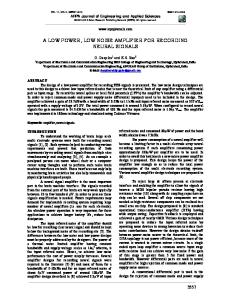
REV B www.wantcominc.com b) Passband Frequency Response As shown in Figure 1, the typical gain of the WHM0110AE is from 18.0 dB to 22.5 dB across 0.1 GHz to 1.1 GHz. The typical input and output return losses are 20 dB and 18 dB across the frequency of 0.1 to 1.1 GHz. The return losses and gain are usable up to 2.0 GHz. Figure 2 shows the full band performance up to 2.0 GHz. Figure 3 shows the measured P1dB and IP3 of the WHM0110AE. The typical P1dB and IP3 are 17 dBm and 34 dBm in the frequency range of 0.10 GHz to 2.0 GHz, respectively. Figure 4 illustrates the measured noise figure performance at full temperature. The measured results include the test fixture loss of approximately 0.05 dB to 0.10 dB depending on the frequency. The noise figure is 0.60 dB to 0.75 dB across the frequency range of 0.1 to 1.1 GHz at room temperature. The noise figure is below 1.0 dB at 2.0 GHz. At 85 0C, WHM0110AE only has 0.35 dB noise increases. At –40 0C, WHM0110AE offers approximately 0.25 dB less noise figure than that at room temperature. Figure 5 demonstrates the stability factor k of the amplifier. The k values are slightly below 1 in some frequency ranges of 2.7 GHz to 3.4 GHz. Figure 6 plots the input and output stability circles. As shows in Figure 6, the red circles are the input stability circles and there are some small potential unstable areas falling into the unit Smith Chart. The high inductance to open load would cause the unstable to the amplifier. The blue circles are the output stability circles and there are some small potential unstable areas falling into the unit Smith Chart. The high capacitance to open load would cause the unstable to the amplifier. Figure 7 is the block diagram of internal circuit of WHM0110AE. It is one stage amplifier with the DC block capacitors at the input and output RF ports. All the RF matching networks, DC bias circuitries, and temperature compensation circuits are built in. Figure 8 demonstrates the application schematic diagram of WHM0110AE. It requires two (2) external decoupling capacitors of 0.01 uF to build a LNA with WHM0110AE. The +5V DC can be applied either at Pin 3 or Pin 5 depending on the availability of the +5.0V source location. No DC block capacitor is required for both input and output RF ports. For +5V line trace length being longer than 6 inch without a decoupling capacitor, an additional 0.01 ~ 0.1 uF de-coupling capacitor with minimum rating voltage of 10V may be needed across the +5V line to ground. The capacitor must be rated in the temperature range of -40 0C to 85 0C to ensure the entire circuit working in the specified temperature range. Figure 9 shows the mechanical outline and recommended motherboard layout of WHM0110AE. Plenty of ground vias on the motherboard are essential for the RF grounding. The width of the 50-Ohm lines at the input and output RF ports may be different for different property of the substrate.
WHM0110AE Performance @ 25 C
25 20
20
15
15
10 S11
5
S21
S12
10
S22
S11
5
Sij (dB)
Sij (dB)
WHM0110AE Performance @ 25 C
25
0 -5 -10
S21
S12
S22
0 -5 -10
-15
-15
-20 Freq (GHz)
-25 0.1
0.2
0.3
0.4
0.5
0.6
0.7
0.8
0.9
1.0
1.1
1.2
-20 Freq (GHz)
-25 0.0
FIG. 1 Typical small signal performance.
0.2
0.4
0.6
0.8
1.0
1.2
1.4
1.6
1.8
2.0
FIG. 2 Small signal performance up to 2 GHz.
2
REV B www.wantcominc.com WHM0110AE IP3 and P1dB
WHM0110AE Noise Figure
2.0
45
1.8
25C
40
1.6
-40C
35
1.4
30
1.2
NF (dB)
dBm
50
25 20 15
85C
1.0 0.8 0.6
10
IP3 (dBm)
5
P1dB (dBm)
0.4 0.2
Freq (GHz)
0
Freq (GHz)
0.0
0.0
0.2
0.4
0.6
0.8
1.0
1.2
1.4
1.6
1.8
2.0
FIG. 3 Typical P1dB and IP3 at room temperature.
0.0
0.2
0.4
0.6
0.8
1.0
1.2
1.4
1.6
1.8
2.0
FIG. 4 Noise figure performance at full temperature
WHM0110AE Stability Factor k
10 9 8 7
k
6 5 4 3 2 1 Freq (GHz)
0 0.0
0.5
1.0 1.5
2.0
2.5
3.0 3.5
4.0
4.5
5.0 5.5
6.0
FIG. 5 Measured stability factor k
FIG. 6 Plots of Input and output stability circles
FIG. 5 Block diagram of internal circuit.
FIG. 6 Typical application schematic for WHM0110AE
3
REV B www.wantcominc.com
WHM0110AE Mechanical Outline, WHM-1:
FIG. 7 WHM0110AE outline
Ordering Information Model Number
WHM0110AE
Waffle pack with the capacity of 100 pieces (10 x 10) is used for the packing. Contact factory for tape and reel packing option for higher volume requirements.
4
REV B www.wantcominc.com
Small Signal S-Parameters: !WHM0110AE !s-parameters at Vds=5V, Id=60 mA, including the test board. !Last updated 2/2/04. # GHZ s MA R 50 !F(GHz)
MAG S11 ANG S11 MAG S21 ANG S21 MAG S12 ANG S12 MAG S22 ANG S22
0.05 0.1 0.2 0.3 0.4 0.5 0.6 0.7 0.8 0.9 1 1.1 1.2 1.3 1.4 1.5 1.6 1.7 1.8 1.9 2 2.1 2.2 2.3 2.4 2.5 2.6 2.7 2.8 2.9 3 3.1 3.2 3.3 3.4 3.5 3.6 3.7 3.8 3.9 4 4.1 4.2 4.3 4.4 4.5 5 5.5 6
0.145 0.086 0.089 0.092 0.098 0.107 0.116 0.120 0.124 0.129 0.130 0.132 0.134 0.134 0.130 0.129 0.129 0.133 0.126 0.077 0.070 0.136 0.180 0.223 0.273 0.319 0.372 0.431 0.495 0.557 0.611 0.649 0.695 0.736 0.779 0.818 0.843 0.855 0.872 0.884 0.892 0.891 0.889 0.887 0.881 0.866 0.800 0.647 0.603
84.5 28.8 -38.1 -73.3 -103.0 -127.0 -149.6 -169.6 172.4 154.9 139.7 124.7 111.5 98.2 88.3 77.7 68.0 58.0 43.2 28.7 85.3 75.2 65.2 53.4 41.8 29.2 16.4 2.9 -11.3 -26.7 -43.1 -57.9 -71.6 -86.4 -101.4 -115.9 -130.6 -145.0 -159.0 -172.2 173.9 160.6 147.6 134.8 121.8 109.2 47.1 -16.7 -64.2
11.941 12.072 13.016 12.629 12.125 11.517 10.873 10.268 9.669 9.088 8.560 8.072 7.622 7.220 6.859 6.546 6.210 5.868 5.442 5.224 5.246 4.846 4.512 4.277 4.030 3.820 3.597 3.330 2.998 2.649 2.290 2.177 2.076 1.829 1.550 1.283 1.062 0.875 0.711 0.567 0.444 0.336 0.253 0.182 0.121 0.072 0.063 0.081 0.049
-140.5 -161.5 163.9 144.1 127.4 112.4 98.3 85.0 72.3 60.1 48.3 36.7 25.2 13.9 3.1 -7.8 -19.0 -30.2 -40.9 -49.3 -61.7 -74.9 -85.2 -96.1 -108.0 -120.2 -132.0 -143.2 -155.6 -168.2 -177.8 174.6 160.2 145.2 132.9 121.3 110.3 99.7 90.3 81.4 72.9 64.1 55.2 47.5 42.7 40.4 150.5 108.9 60.0
0.0440 0.0480 0.0510 0.0520 0.0550 0.0570 0.0600 0.0640 0.0680 0.0730 0.0770 0.0820 0.0870 0.0920 0.0970 0.1030 0.1080 0.1140 0.1200 0.1270 0.1270 0.1230 0.1280 0.1320 0.1370 0.1400 0.1390 0.1370 0.1370 0.1330 0.1230 0.1170 0.1190 0.1180 0.1100 0.1040 0.0990 0.0960 0.0910 0.0850 0.0810 0.0790 0.0770 0.0730 0.0690 0.0660 0.0500 0.0610 0.0770
57.3 33.4 13.9 8.3 4.6 1.5 -1.6 -5.0 -8.9 -13.1 -17.9 -23.0 -28.2 -34.1 -40.1 -46.4 -53.1 -60.6 -68.3 -76.1 -89.3 -94.2 -100.4 -108.7 -117.6 -126.8 -136.4 -147.5 -158.7 -169.2 -178.7 175.0 165.8 155.2 145.3 135.5 125.5 115.9 107.0 97.0 85.6 74.4 65.5 56.0 44.3 32.9 -13.2 -48.1 -83.0
0.124 0.123 0.114 0.116 0.113 0.108 0.107 0.103 0.101 0.100 0.100 0.104 0.110 0.114 0.129 0.141 0.154 0.167 0.178 0.199 0.302 0.321 0.354 0.393 0.432 0.472 0.514 0.557 0.600 0.640 0.651 0.612 0.692 0.763 0.802 0.834 0.857 0.874 0.887 0.897 0.908 0.917 0.926 0.932 0.936 0.938 0.940 0.938 0.929
-178.9 167.3 134.6 107.2 79.6 55.7 31.5 7.3 -15.7 -38.3 -61.9 -83.6 -106.3 -126.2 -145.7 -164.9 177.1 160.8 147.1 142.0 128.8 106.2 92.3 78.3 64.9 51.4 38.6 25.5 12.6 -1.4 -16.1 -23.7 -30.0 -42.6 -55.1 -67.0 -79.0 -90.2 -101.1 -111.3 -121.4 -131.6 -141.0 -150.8 -160.0 -169.4 147.0 104.6 64.4
5