Физика и техника полупроводников, 1999, том 33, вып. 9
Quantum dots: paradigm changes in semiconductor physics © D. Bimberg Institute fur ¨ Festkorperphysik, ¨ Technische Universitat ¨ Berlin, 10623 Berlin, Germany
(Получена 1 марта 1999 г. Принята к печати 2 марта 1999 г.) Deposition of one to a few monolayers of a semiconductor having a lattice constant largely different from the underlying substrate leads to formation of coherent ”quantum dot arrays” of densities beyond 1011 cm−2 in a matter of seconds. Self-organisation effects govern their massively parallel formation. Fundamental paradigms of semiconductor physics have to be changed in describing such quantum dots or their ensembles.
1. Introduction Resent breakthroughs in solid state physics are related to the fast development of the new classes of structures — self-organized quantum dots (QDs). These unique objects combine advantages of a bulk semiconductor with those of single atoms. Their physical properties resemble an atom in a cage. It is possible to touch a semiconductor quantum dot with a tip of a scanning tunneling microscope, inject charged carriers and monitor emission from a single QD, and realize many other unique experiments. Interaction of carriers in QDs is defind completely by the laws of quantum mechanics and no ”motion” of carriers is possible in a traditional sense. The main mechanism of the information transfer between QDs becomes single electron tunneling and Coulomb interaction of carriers in neighbouring dots. These give rise to novel directions in microelectronics: single electronics and quantum dot cellular automata computing. QDs allow significant improvements of characteristics of many modern devices: e. g. infrared detectors, light-emitting diodes, lasers, solar cells. Since the first experimental [1] and theoretical [2,3] papers on QDs, some fundamental understanding of their physical properties, their growth and their device relevance has been obtained [4–6].
2. Electronic spectrum of a quantum dot To understand the reasons for the unique properties of QDs let us first refer to the electronic spectrum of a 3D solid. It is well known that a single atom has discrete energy levels separated by forbidden energy gaps, as shown in Fig. 1. When an atom is excited, the electron goes to the higher energy level, and when it relaxes back to the ground state, a photon with strictly defined energy is emitted. The width of the emission or absorption line (∆E) is defined by the fundamental relation with the lifetime of the electron in the upper state. The uncertainty in the emitted energy is: τ ∆E > ~,
(1)
where τ is the total lifetime of the electron in the excited state. In contrast to the case of a diluted gas of atoms, the atoms in crystals are strongly bound to each other. Their high density in crystals plays a very important role in
modern solid-state devices allowing high absorption or (in case of population inversion) gain coefficients, providing high conductivity and making possible high density flows of charged carries through the crystal. Due to this, a modern semiconductor laser having the length of 1 mm and the crosssection of 10−4 mm2 can emit continuous light with power of several watts, while a corresponding gas laser has several meter long size. At the same time, small separations between atoms makes interaction of their electron levels unavoidable. This interaction results in formation of wide bands of allowed states in contrast to the discrete (δ-function-like) energy spectrum of single atoms. In semiconductors, the last filled band of allowed states is called ”valence band” and the next empty band is called ”conduction band”. Due to the broad spectrum of allowed states in these bands, a wide range of transition energies between electrons from the filled valence band to empty states in the conduction band is possible. The absorption band becomes rather broad of the order of several electron volts, in marked difference with sharp line absorption spectrum of single atom. The excited electrons in the conduction band, as well as the empty states in the valence band (”holes”) can move in the crystal via tunneling between sites of the crystal lattice. As the atom potential profile in a crystal is periodic, electrons and holes can move freely through the crystal, as free cattiers do in vacuum. However, the motion of charged carriers in crystals is described by a mass different of that of free electrons, defined by the crystal field. The carriers are thus called ”quasiparticles”. In the widely used optoelectronic III–V materials (gallium arsenide — GaAs; indium arsenide — InAs, etc.), the electrons effective masses are in the range of 0.01÷0.1 of the electron mass in vacuum. Wide bands of allowed states in the crystal provide a lot of possibilities for scattering of electrons and holes. Lattice vibrations easily stimulate transitions of charge carriers in the energy range defined by the lattice temperature and / or scatter their direction. The tails of the carrier distribution near the bottom of the conduction band and the top of the valence band increase remarkably with temperature. Thus, the concentration of carriers per energy interval near the bandedge drops. For the same concentration of injected carriers broadening of their energy spectra results, among
1044
Quantum dots: paradigm changes in semiconductor physics
1045
Figure 1. Schematic representation of energy levels in a single atom, a bulk semiconductor and a quantum dot.
other disadvantages, leading to the decrease in maximum gain and degradation of laser performance. The situation changes remarkably, if the motion of the charged carrier in the crystal is limited to a very small volume, e. g. in a three-dimensional rectangular box. Localization of carriers can be provided by a surrounding (matrix) material. In the laser case it is important that the matrix material has a larger bandgap than the box material and that the potential wells are attractive both for electrons and holes. As an electron shows properties of both a particle and a wave, if the size of the box is small, the electron energy spectrum is quantized similar to the case of the electron quantization in the attracting Coulomb potential of a nuclei. In a simplified case of infinite barriers at the box-matrix interface, the size quantization energy is described by: Ex,y,z
~2 = 2m∗e
�
πn Lx,y,z
�2 ,
(2)
where m∗e is the electron effective mass, Ex,y,z is the size quantization energy due to electron localization in the box with dimensions Lx , Ly , and Lz , sespectively, and n = 1, 2, 3, . . . . Физика и техника полупроводников, 1999, том 33, вып. 9
Electrons in crystals usually have rather small effective mass, and, an already large size of the box of about 10 nm can result in a large energy separation between electron sublevels (about 100 meV for GaAs QD). The latter value significantly exceeds the thermal energy at room temperature (26 meV), and, thus, population of excited states can be avoided. In this sense there will be no temperature dependence of the optical spectrum of such box in a wide temperature range, and the realization of temperature insensitive devices becomes possible.
3. Self-organized growth of QDs Until recently there was a lack of ideas how to realize QDs with size and uniformity required for applications and compatible to modern semiconductor technology. Traditional methods based on patterning of structures with ultrathin layers suffered either from insufficient lateral resolution, or introduced heavy damage in the material upon processing. There were also predictions that, even if ideal QDs could be fabricated, they can be hardly used for real devices, as ultralong relaxation times between electron sublevels were expected.
D. Bimberg
1046
The breakthrough how to fabricate QDs with requested properties came by using an effect which is traditionally considered as undesirable by crystal growers. It was found that, if one deposits a layer of a material having a different lattice constant with the substrate, the growth of a strained material first proceeds in a planar mode, a ”wetting” layer is formed. However, at some critical thickness this planar growth is followed by a Stranski–Krastanow mode. Threedimensional nanoscale islands are formed on surfaces, as was demonstrated first for the case of growth of indium arsenide on gallium arsenide in 1985 by a group at CNET, France [5]. When these islands are covered with GaAs, a GaAs ”pie” with InAs ”raisins” is formed. As InAs has a much smaller bandgap than GaAs, an array of InAs QDs is formed. Initially this technique did not take much attention since the possibility to produce QDs uniform in size and shape and dislocation-free was not realized. The driving force for the formation of three-dimensional islands is related to elastic strain relaxation. The material on top of the pyramid can relax elastically expanding in vacuum, giving rise to significant energy benefit. For 45◦ facet angle of the pyramid, 60% of the elastic energy accumulated in the biaxially compressed flat layer is relaxed [6,7]. On the other hand, formation of pyramids results in an increase of the total surface area. If formation of islands results in an increase of the surface energy of the system, the initially formed islands will undergo ripening, as the system will try to reduce the total surface area covered by QDs. A possibility for fabrication of QDs uniform in size and shape, being stable with respect to ripening appears only if the total surface energy of the island is smaller than the surface energy of the corresponding area of the wetting layer occupied by it. If one takes into account that the major surface properties, e. g. surface reconstruction, surface stress etc., are strongly affected by the strain state of the crystal, one can conclude that they can differ significantly for the strained wetting layer and the facet of the relaxed pyramid. Numerical estimates of the strain–induced renormalization of the surface energy made by Shchukin et al [7], indicate that formation of ”equilibrium”, equisized and equishaped islands which do not undergo ripening is probable. Optimization of growth parameters to realise equilibrium arrays is a difficult task to be solved for each material system separately [8]. If islands uniform in size and in shape are formed, one speaks of ”self-organized quantum dots”, as this system represents a clear example of spontaneous formation of macroscopic order from initially random distributions. In the case of dense arrays of QDs, their interaction via the strained substrate makes their lareral ordering favorable [7]. Growth on patterned surfaces can also led to ordered QDs [9]. For multi-stack QD deposition vertically-correlated growth of QDs has been demonstrated [5,8] and, thus, quasicrystals composed of quantum dots either in two or in all three dimensions can be fabricated. For islands having a two-dimensional shape either correlated or anticorrelated growth is possible depending on the relative thichness of the spacer layer [10].
4. Proof of electronic quantum dot An important breakthrough in understanding the electronic properties of semiconductor QDs occurred when it was demonstrated that ultranarrow luminescence lines from single InAs QDs [11,12] exhibit no broadening with temperature [13], a very unusual phenomenon for any electron– hole emission in semiconductors, in a full agreement with theoretical predictions for electronic QDs (see Fig. 2).
Figure 2. Ultrasharp luminescence lines from single QDs at 20 K (a) which do not show broadening with temperature increase (b).
A lot of progress has been achieved in the last few years, more than in decades of previous reseach. We have learned about QDs in different materials systems, about the electron spectrum in type-II QDs, radiative recombination and relaxation processes. Numerous teams contributed to the development of this subject. Among them Ioffe Institute, CNET, UCSB, USC, Stanford, Lund, Sheffield and Nottingham Universities, Max-Planck Institute in Stuttgart and many other groups and institutions.
5. Single electronics Single electronics is based on quantum effects related to the charging of QDs and tunneling of carriers through it. If the ground state of a QDs is not occupied, external electrons can tunnel to this level. If the QD ground state is occupied with one electron, an additional energy Физика и техника полупроводников, 1999, том 33, вып. 9
Quantum dots: paradigm changes in semiconductor physics
1047
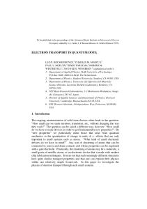
Figure 3. STM image of free-standing InAs QDs of Si (100) surface (a) and high-resolution transmission electron microscopy image of Si-covered coherent InAs QDs in Si matrix (b).
is necessary to put another electron in the QD, because of the Coulomb repulsion with the existing electron. This ”Coulomb blocade” regime makes it possible to realize principally new logics and operational principles for further generations of microelectronic circuits.
based on QWs. Reduction of the depopulation rate of upper sublevels [15] in view of the necessity of multi-phonon emission to fit the intrasublevel energy in property designed QDs results in much better probability to create population inversion for intrasublevel transitions in QDs.
6. Quantum dot molecules. Quantum dot cellular automata
9. Light emitters
If QDs are placed together forming a cell having welldefined symmetry and allowing ”switching of carriers” between two or more energetically equivalent positions in the cell, and these cells are combined in a network, a new concept for construction of integrated circuits appears. In this case it is not the current which carries the information, but the polarization of the QD chain, or of the QD molecule. In principle the operation of such a molecule can be made practically energy dessipation-free, and the information propagates at the speed of electromagnetic waves [14].
7. Data storage Ultrahigh area density of QDs and potentially very high localization energy of carriers in QDs make possible the realisation of a new generation of memory devices. QDs can be also made of magnetic materials, or serve as an active media in photon-memory devices.
8. Far-infrared detectors and emitters Size quantization of carriers in all three dimensions results in lifting of k-selection rules prohibiting intrasubband absorption in quantum wells (QWs) for the light propagating perpendicular to the surface of the wafer. This makes QD far-infrared detectors advantageous with respect to those Физика и техника полупроводников, 1999, том 33, вып. 9
Electron and hole overlap is close to unity in a QD. Together with the lifting of the k-selection rule for radiative annihilation of excitons, and the lack of screening of Coulomb interaction between electrons and holes, this results in ultrahigh material gain in a QD. The material gain is also inversely proportional to the QD volume, and dense arrays of very small QDs can result in maximum gain of the order of 105 cm−1 . Such high gain affects the refractive index in the vicinity of the absorption / gain resonance resulting in a strong photon energy dependent oscillatory variation of refractive index, leads to resonant waveguiding without a heterostructure [16,17]. No Fermi function describes the statistical properties of a QD ensemble, like carrier distribution. Master equations of microstates describe static and dynamic properties like gain, capture, recombination . . . [18]. High temperature stability of threshold current in a QD laser is demonstrated [19] in agreement with the theoretical predictions, and theoretical understanding of the QD laser has been achived [20,21]. Competitive edge- [22–24] and surface-emitting [25] lasers are created.
10. New challenges in heteroepitaxy: InAs quantum dots in Si Another field, where application of QDs can play an extraordinary role, is related to silicon. Silicon being the major material for modern microelectronics provides very
D. Bimberg
1048
low probability for injected electrons and holes to recombine radiatively, and can be hardly used in lasers and lightemitting devices. If it is possible to insert narrow-gap QDs (e. g. made from InAs) which have high probability of radiative recimbination in such a way that electrons and holes will be trapped in these QDs, a silicon-based device with extremely efficient radiative recombination can be created. Recently, a possibility to deposit such InAs quantum dots on Si surface was demonstrated [26]. A scanning tunneling microscopy image of free-standing InAs QDs on a silicon (100) surface and a high-resolution transmission electron microscopy image of siliconovergrown InAs QDs are presented in Fig. 3, a and b, respectively. Coherent InAs QDs in a silicon matrix demonstrate broad photoluminescence band peaking at 1.3 µm at 77 K and at 1.6 µm at 300 K. New generations of photonic and electronic devices based on quantum dots are emerging presently, revolutionising semiconductor technology and industry. Acknowledgments: I am very grateful to N.N. Ledentsov for his help, to Volkswagen Foundation, INTAS, DFG and BMBF for financial assistance.
References [1] A.I. Ekimov, A.A. Onushzhenko. JETP Lett., 34, 2225 (1981). [2] Al.L. Efros, A.L. Efros. Sov. Phys. Semicond., 16, 772 (1982). [3] Y. Arakawa, H. Sakaki. Appl. Phys. Lett., 40, 939 (1982); M. Asada, M. Miyamoto, Y. Suematsu. IEEE J. Quant. Electron., QE-22, 1915 (1986). [4] D. Bimberg, M. Grundmann, N.N. Ledentsov. Quantum Dot Heterostructures (J. Wiley, 1998). [5] L. Goldstein, F. Glas, J.Y. Marzin, M.N. Charasse, G. Le Roux. Appl. Phys. Lett., 47, 1099 (1985). [6] M. Grundmann, O. Stier, D. Bimberg. Phys. Rev. B, 51, 11 969 (1995); O. Stier, M. Grundmann, D. Bimberg. Phys. Rev. B, in print. [7] V.A. Shchukin, N.N. Ledentsov, P.S. Kop’ev, D. Bimberg. Phys. Rev. Lett., 75, 2968 (1995); V.A. Shchukin, D. Bimberg. Rev. Mod. Phys. (1999), in print. [8] N.N. Ledentsov, M. Grundmann, N. Kirstaedter, O. Schmidt, R. Heitz, J. B¨ohrer, D. Bimberg, V.M. Ustinov, V.A. Shchukin, P.S. Kop’ev, Zh.I. Alferov, S.S. Ruvimov, A.O. Kosogov, P. Werner, U. Richter, U. G¨osele, J. Heydenreich. Proc. MSS7, (1995) [Sol. St. Electron., 40, 785 (1996)]. [9] T.T. Ngo, P.M. Petroff, H. Sakaki, J.L. Merz. Phys. Rev. B, 53, 9618 (1996). [10] V.A. Shchukin, D. Bimberg, V.G. Malyshkin, N.N. Ledentsov. Phys. Rev. B, 57, 12 262 (1998). [11] N.N. Ledentsov, M. Grundmann, N. Kirstaedter, J. Christen, R. Heitz, J. B¨ohrer, F. Heinrichsdorff, D. Bimberg, S.S. Ruvimov, P. Werner, U. Richter, U. G¨osele, J. Heydenreich, V.M. Ustinov, A.Yu. Egorov, M.V. Maximov, P.S. Kop’ev, Zh.I. Alferov. Proc. 22nd Int. Conf. Phys. Semicond. (Vancouver, 1994), ed. by D.J. Lockwood (World Scintific, Singapore, 1995) v. 3, p. 1855. [12] J.-Y. Marzin, J.M. Gerard, A. Izra¨el, D. Barrier, G. Bastard. Phys. Rev. Lett., 73, 716 (1994).
[13] M. Grundmann, J. Christen, N.N. Ledentsov, J. B¨ohrer, D. Bimberg, S.S. Ruvimov, P. Werner, U. Richter, U. G¨osele, J. Heydenreich, V.M. Ustinov, A.Yu. Egorov, A.E. Zhukov, P.S. Kop’ev, Zh.I. Alferov. Phys. Rev. Lett., 74, 4043 (1995). [14] C.S. Lent, P.D. Tuogaw, W. Porod. Appl. Phys. Lett., 62, 714 (1993). [15] H. Benisty, C.M. Sotomayor Torres, C. Weisbuch. Phys. Rev. B, 44, 10 945 (1991); T. Inoshita, H. Sakaki. Phys. Rev. B, 46, 7260 (1992). [16] N.N. Ledentsov, I.L. Krestnikov, M.V. Maximov, S.V. Ivanov, S.L. Sorokin, P.S. Kop’ev, Zh.I. Alferov, D. Bimberg, C.M. Sotomayor Torres. Appl. Phys. Lett., 69, 1343 (1996). [17] I.L. Krestnikov, M.V. Maximov, A.V. Sakharov, P.S. Kop’ev, Zh.I. Alferov, N.N. Ledentsov, D. Bimberg, C.M. Sotomayor Torres. J. Cryst. Growth, 184/185, 545 (1998). [18] M. Grundmann, D. Bimberg. Phys. Rev. B, 55, 4181 (1997). [19] N. Kirstaedter, N.N. Ledentsov, M. Grundmann, D. Bimberg, V.M. Ustinov, S.S. Ruvimov, M.V. Maximov, P.S. Kop’ev, Zh.I. Alferov, U. Richter, P. Werner, U. Gosele, H. Heydenreich. Electron Lett., 30, 1416 (1994). [20] L.V. Asryan, R.A. Suris. IEEE J. Select. Topics Quant. Electron,. 3, 148 (1997). [21] M. Grundmann, D. Bimberg. Japan. J. Appl. Phys., 36, 4181 (1997). [22] N.N. Ledentsov, V.A. Shchukin, M. Grundmann, N. Kirstaed¨ ter, J. Bhrer, O. Schmidt, D. Bimberg, S.V. Zaitsev, V.M. Ustinov, A.E. Zhukov, P.S. Kop’ev, Zh.I. Alferov, A.O. Kosogov, S.S. Ruvimov, P. Werner, U. G¨osele, J. Heydenreich. Phys. Rev. B, 54, 8743 (1996). [23] F. Heinrichsdorff, M.-H. Mao, A. Krost, N. Kirstaedter, D. Bimberg, A.O. Kosogov, P. Werner. Appl. Phys. Lett., 71, 22 (1997). [24] M.V. Maximov, Yu.M. Shernyakov, A.F. Tsatsul’nikov, A.V. Lunev, A.V. Sakharov, V.M. Ustinov, A.Yu. Egorov, A.E. Zhukov, A.R. Kovsh, P.S. Kop’ev, L.V. Asryan, Zh.I. Alferov, A.O. Kosogov, P. Werner. J. Appl. Phys. 83, 5561 (1998). [25] J.A. Lott, N.N. Ledentsov, V.M. Ustinov, A.Yu. Egorov, A.E. Zhukov, P.S. Kop’ev, Zh.I. Alferov, D. Bimberg. Electron Lett., 33, 1150 (1997). [26] G.E. Cirlin, V.N. Petrov, V.G. Dubrovsky, S.A. Masalov, A.O. Golubok, N.I. Komyak, N.N. Ledentsov, Zh.I. Alferov, D. Bimberg. Tech. Phys. Lett., 24, (8), 10 (1998); A.F. Tsatsul’nikov, A.Yu. Egorov, P.S. Kop’ev, A.R. Kovsh, M.V. Maximov, N.A. Bert, V.M. Ustinov, B.V. Volovik, A.E. Zhukov, Zh.I. Alferov, G.E. Cirlin, A.O. Golubok, S.A. Masalov, V.N. Petrov, N.N. Ledentsov, R. Heitz, M. Grundmann, D. Bimberg, I.P. Soshnikov, P. Werner, U. G¨osele. Proc. ICPS 24 (Jerusalem, 1998) (World Scientific, 1998). Редактор Л.В. Шаронова
Физика и техника полупроводников, 1999, том 33, вып. 9