Implementation of a Streaming Camera using an FPGA and CMOS Image Sensor
Daniel Crispell Brown University
1. Introduction Because of the constantly decreasing size and cost of image sensors and increasing complexity of FPGA circuits, it has become feasible to implement a compact streaming video camera using these two components. Because of the flexibility and reprogrammability of the FPGAs, additional functionality may be implemented, using the streaming camera as a base. This document describes the construction of a streaming video camera using a Xilinx Spartan-II FPGA and a National Semiconductor LM9618 CMOS Image Sensor. 2. Problem Formulation The goal of this project is to construct a small camera system capable of streaming live video images from a CMOS image sensor to a PC through the parallel port interface provided on the Xilinx XSA FPGA development board. The project is to serve as an introduction to hardware design using VHDL, as well as provide a starting point for future applications involving the camera. The camera should be capable of handling up to 30 frames per second of VGA resolution images from the sensor, but due to the constraints imposed by the parallel port may transfer data to the host PC at a much lower rate. 3. Method of Solution 3.1 Image Sensor The image sensor used is a National Semiconductor LM9618 CMOS Image Sensor. Its flexibility and ease of use makes it a good choice for the system. Its data bus can be configured as 12, 10 or 8 bits wide, and it has a moveable and resizable frame of view. All functionality is controlled via internal registers which are accessed via an I2C bus. National Semiconductor also provides a headboard for the sensor, which allows a lens to be attached and provides easy access to the necessary control and data lines.
Figure 1: National LM9618 headboard, with and without lens attachment
3.2 FPGA / Development Board
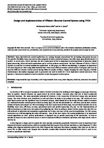
The XESS XSA development board is used to prototype and test the design. The board is built around a Xilinx Spartan-II XC2S100 FPGA. The board also contains 16 MB of external RAM memory in the Hynix HY57V281620A chip, as well as 256 KB of flash memory. The on-board CPLD and parallel port interface makes it easy to load new designs into the FPGA. The board also provides several useful components for input/debugging such as a pushbutton, dip switches, etc. 3.3 VHDL Implementation The software placed in the FPGA is implemented in VHDL. VHDL provides strong type checking and allows us to build the design up from smaller modules. The program loaded onto the FPGA has three main tasks: to control the CMOS image sensor, to read and store pixel data from the CMOS image sensor, and to stream the pixel data to the host software through the parallel port. The software is divided into several modules, each performing a specific function. Below is a block diagram of the data flow within the system.
LM9618
Host PC
pixel data
pixel data (parallel port)
PP Controller
Pixel Packer packed pixel data
FIFO In FIFO status
packed pixel data
Traffic Controller
FIFO Out FIFO status
memory control pixel data to memory
pixel data from memory
SDRAM
Figure 2: System dataflow block diagram
3.3.1 I2C Interface The I2C interface is made up of two modules. The lowest-level module is the “simple_i2c” component. This component is a bare-bones I2C interface available from http://www.opencores.com. Build on top of that module is the “lm9628_i2c_interface” module, which is based on a Dallas 1621 interface written by Richard Herveille, also available from opencores.com. The module provides an address, data, and several control lines for reading and writing values to registers via the I2C bus. The top-level module (the stream_camera_top component) utilizes this interface in order to initialize the CMOS sensor with the correct settings in its control registers. 3.3.2 Storing Pixel Data The first step in storing images from the camera is to receive two eight bit pixels and store them in a single sixteen bit word. This is accomplished in the pixel_packer component. Once two pixels are received from the sensor, they are passed to a FIFO buffer in the form of a single word, with the first pixel received stored in the lower 8 bits and the second pixel in the upper 8 bits. The output data lines of the FIFO are connected to the input data lines of the memory interface, and the FIFO status signals are fed to the memory arbitration unit. The memory arbitration unit (the traffic_controller component) controls access to the memory interface. 3.3.3 Streaming Pixel Data The camera utilizes the parallel port to communicate with the host PC. Because of the way the interface CPLD is programmed on the XSA development board, there are seven bits available for data from the PC to the FGPA (commands) , and four status bits available for data from the FPGA to the PC (image data). The pp_interface module controls the movement of data in and out of the parallel port at the lowest level. The lsb of the seven bit data bus is debounced by the signal_debounce component and used as the clock for the synchronous transfer of image data from the FPGA to the PC. Because only one nibble (4 bits) can be sent from the FPGA at a time, a second clock is generated that transitions with a rising edge every time the transfer of one sixteen bit word is complete. This allows the remaining layers of software to be unaware of the four bit limitation and transfer one full word at a time. The pp_controller module is one layer above the pp_interface module. Its main function is to read incoming commands from the PC and initiate frame transfers when appropriate. It provides a status signal to the memory arbitration unit as well to indicate when a frame is being transferred and pixel data from memory is needed.
3.3.4 Memory Arbitration / Control Logic
Because the modules responsible for both outgoing and incoming data need access to the memory, some sort of arbitration is needed. The incoming and outgoing transfer rates are very different and not synchronized in any way, so in order to guarantee that we have a complete image to transfer at any given time, we need three separate image buffers. We need one buffer to hold the incoming pixel data, one buffer to hold the pixel data of the outgoing image, and one buffer to hold the last complete frame. These details are handled by the traffic_controller module. The module transfers data two pixels (one 16-bit word) at a time to both the input and output FIFO’s. If no frame is currently being outputted through the parallel port and there is data to be read in the incoming FIFO, that data is read and stored in memory. If there is a frame currently being output through the parallel port, the module writes data to the outgoing FIFO until it asserts its “almost full” status flag. Because the speed of the memory is very fast in comparison to the speed at which data can be transferred over the parallel port, the system has no problem keeping up. Finally, if the outgoing FIFO is sufficiently full and the incoming FIFO contains new data, it is read and stored in memory. Each of the three frame buffers in memory has a unique address offset, making it simple for the traffic_controller module to switch between them. When a request for a new frame is received from the host, the offsets for the last complete frame and outgoing frame are swapped, so that the latest frame is transferred to the host. When the start of a new frame is received from the camera, the incoming and last complete frame offsets are swapped. On the rare occasion that the two events occur during the same clock cycle, the outgoing and incoming buffer offsets are swapped. Using this logic, we guarantee that incoming and outgoing images are never corrupted with data from other frames.
3.4 External Connections Below is a wiring diagram of the external connections between the XSA development board and the CMOS sensor headboard. Note that the I2C pins SDA and SCLK must be tied to +3.3V with a pull-up resistor. Also, because the implementation uses only 8 bits per pixel, data lines D0, D1, D2, and D3 are unconnected.
Figure 3: External Connections
3.5 Host Software The host software’s main function is to retrieve image data from the sensor and display the data in the form of a streaming video. The front end for the system is written in the Java programming language because of the ease with which graphical user interfaces can be programmed in it. Unfortunately, a satisfactory parallel port interface could not be obtained, so that portion of the system is written in C, and interfaced to the Java front end via the Java Native Interface (JNI). The main class, StreamCameraApp, simply instantiates the VideoStreamGUI class, which is an extension of the JFrame class. To store the image data, the MemoryImageSource class is used, allowing direct access to the raw image data and easy updating of the display. The VideoStreamGUI class provides a frame for the image to be shown, and creates and starts an instance of the FrameUpdateThread class. This is where the GUI interfaces with the native code
and pixel data is retrieved. The process of reading in a frame is encapsulated in the readFrame() native function. This involves a “start transfer” command being issued over the parallel port, followed by the reading in of the frame width, height, and pixel data. The pixel data is read one word at a time, with two 8-bit pixel values stored per 16bit word, so it must be unpacked and stored in the appropriate data structure for display. In this case, one 32 bit word is used per pixel, with 8 bits allocated each to the alpha, red, green, and blue components. The grayscale intensity value is stored in each of the red, green, and blue components, along with an alpha value of 255 (max). Once the new data is stored, MemoryImageSource.newPixels() is called and the display is automatically updated.
Figure 4 : A screenshot of the host interface
4. Results and Discussion Because the inherent bandwidth issues that come with transferring streaming video over the parallel port, the system is limited to small images with relatively low frame rates. For example, using a frame size of 200x150, a frame rate of about 3 fps can be achieved. This equates roughly to a bit rate of 720 kilobits per second. The images themselves, although made small to achieve a somewhat reasonable frame rate, are of relatively good quality. For single image acquisition, or if the images do not need to be streamed over the parallel port, the full 640x480 resolution of the sensor can be used.
5. Conclusion and Further Work One of the goals of this project was to create an FPGA-based camera system that future projects could serve as a starting point for future projects. Possibly the simplest improvement that could be made to this design would be to allow for the display of color images. Because National Semiconductor produces an identical CMOS sensor with a Bayer Pattern color mosaic (LM9628), the RGB image planes could be produced within the host software and a color image could be displayed. A more advanced improvement would be the implementation of some image processing algorithms within the FPGA. In the current system the pixels are simply read from the sensor and stored to memory, but it is easy to imagine a similar system in which some type of processing is performed on the image data before (or after) it is written to memory. The parallel nature of the FPGA allows algorithms to be run in real time, providing a huge advantage over CPU-based systems, where this might not be possible.
Click below to find more Mipaper at www.lcis.com.tw
Mipaper at www.lcis.com.tw