Digital Logic: From Transistors to Gates Textbook Chapter 3
The Transistor
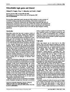
Transistor: building block of computers Microprocessors contain tons of transistors AMD 6-core Opteron (2009): 904 million Intel Core i7 Quad (2008): 731 million Intel Core 2 Duo (2006): 291 million Intel Itanium 2 (2003): 220 million Intel Pentium 4 (2000): 42 million IBM PowerPC 750FX (2002): 38 million IBM/Apple PowerPC G5 (2003): 58 million Intel 4004 (1971): 2300
CMPE12 – Fall 2009
01-2
The Transistor: Past and Present
CMPE12 – Fall 2009
01-3
Moore’s Law “The number of active components per chip will double every 18 months.”
CMPE12 – Fall 2009
01-4
GPU Processing Compared to CPU
CMPE12 – Fall 2009
01-5
What Is a Transistor?
A switch, which can close between the source and the drain Changing the voltage of the gate lets you change the current flow between the source and drain (closing or opening the switch)
CMPE12 – Fall 2009
01-6
Metal-Oxide-Semiconductor transistor
CMPE12 – Fall 2009
01-7
How big is a transistor?
If a CPU die were as big as this whole classroom… A transistor would be…
CMPE12 – Fall 2009
01-8
What is a transistor?
Logically, each transistor is used as a switch Combined to implement logic functions AND,
OR, NOT
Combined to build higher-level structures Adder,
multiplexer, decoder, register, …
Combined to build a processor LC-3,
CMPE12 – Fall 2009
Core 2 Duo, etc
01-9
Simple switch circuit Switch open: No
current through circuit Light is off Vout is +2.9V
Switch closed: Short
Switch-based circuits can easily represent two states: on/off, open/closed, voltage/no voltage. CMPE12 – Fall 2009
circuit across switch Current flows Light is on Vout is 0V 01-10
n-type MOS transistor n-type MOS (nMOS) when Gate has positive voltage, short circuit between #1 and #2 (switch closed) when Gate has zero voltage, open circuit between #1 and #2 (switch open)
Gate = 1
Terminal #2 must be connected to GND (0V).
CMPE12 – Fall 2009
Gate = 0
01-11
p-type MOS transistor p-type is complementary to n-type when Gate has positive voltage, open circuit between #1 and #2 (switch open) when Gate has zero voltage, short circuit between #1 and #2 (switch closed)
Gate = 1
Terminal #1 must be connected to +2.9V in this example.
CMPE12 – Fall 2009
Gate = 0
01-12
Digital Values for Analog Signals
Use the switch behavior of MOS transistors to implement logical functions: AND, OR, NOT Digital symbols: We assign a range of analog voltages to each digital (logic) symbol Assignment of voltage ranges depends on electrical properties of transistors being used
CMPE12 – Fall 2009
01-13
CMOS circuit
CMOS is Complementary Metal Oxide Semiconductor Uses both n-type and p-type MOS transistors p-type (pMOS) Attached to + voltage Pulls output voltage UP when input is zero n-type (nMOS) Attached to GND Pulls output voltage DOWN when input is one
CMPE12 – Fall 2009
01-14
Truth Table
The most basic representation of a logic function It is a perfect induction proof - Lists the output for all possible input combinations How many rows of the truth table needed?
CMPE12 – Fall 2009
Inputs
Outputs
AB…
XY…
2#inputs
01-15
Truth Table: Inverter
Inverted signals are denoted with an overbar Or with a prime symbol A’
CMPE12 – Fall 2009
Input
Output
A
Y = A’
01-16
Inverter (NOT gate)
In
Out
In
Out
0V
2.9 V
0
1
2.9 V
0V
1
0
CMPE12 – Fall 2009
01-17
Truth Table: AND Gate
The result of an AND operation is 1 if and only if all inputs are 1 Depict AND by the multiplication symbol A·B Or by lumping the signals together AB We don’t really build these gates…
CMPE12 – Fall 2009
Inputs
Output
A B
Y=A·B
01-18
NAND gate (NOT-AND)
Note: Parallel structure on top, serial on bottom. CMPE12 – Fall 2009
A 0 0 1 1
B 0 1 0 1
C 1 1 1 0 01-19
AND gate A 0 0 1 1
B 0 1 0 1
C 0 0 0 1
Add an inverter to a NAND.
CMPE12 – Fall 2009
01-20
Truth Table: OR Gate
The result of an OR operation is 1 if and only if any inputs are 1 Depict OR by the addition symbol A+B
CMPE12 – Fall 2009
Inputs
Output
A B
Y=A+B
01-21
NOR Gate: NOT-OR
Note: Serial structure on top, parallel on bottom.
CMPE12 – Fall 2009
A 0 0 1 1
B 0 1 0 1
C 1 0 0 0 01-22
OR gate A 0 0 1 1
B 0 1 0 1
C 0 1 1 1
Add an inverter to a NOR gate.
CMPE12 – Fall 2009
01-23
Truth table to transistors
So giving some arbitrary truth table, how do you go about creating a transistor-based circuit for it? Typically this is only done for a handful of gate types. (ASIC flow vs full custom) Recall:
PMOS (with the bubbles) on top NMOS (no bubbles) on bottom Series structure makes AND Parallel structure makes OR
CMPE12 – Fall 2009
01-24
Synthesis of an AOI Gate
AOI means AND-OR-Invert There are many kinds of these in standard cell libraries
CMPE12 – Fall 2009
01-27
Synthesis of AOI Gate
CMPE12 – Fall 2009
01-28
Why are our circuits so big?
The circuits for the NAND and NOR were a lot smaller than the one we just did. Why is that? We just used the brute force method. To do correctly you need the Function and the dual of the function.