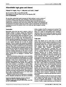
Experiment : LOGIC GATES Object : To verify the truth table of NOT, AND, OR, NOR and NAND gate using RTL (using Resistor Transistor Logic)/ DTL (Diode Transistor Logic)/ Integrated circuits. Apparatus used: Resistor, diode, transistor, LED, 5-volt power supply, IC and connecting wires. Theory: Logic gates: A logic gate is an electronic circuit which makes a logic decision. It has one output and one or more inputs. In other word we can define as “A logic gate is an idealized or physical device implementing a Boolean function, that is, it performs a logical operation on one or more logic inputs and produces a single logic output. Depending on the context, the term may refer to an ideal logic gate, one that has for instance zero rise time and unlimited fan-out, or it may refer to a non-ideal physical device”. The term logic is usually used to refer to decision making process. A logic gate makes logical decision regarding the existence of out put depending upon the nature of input. If we are going to the logic concept then one can understand that answer of any logical statement can be given in terms of True/False or YES/NO. A binary number system has only two numbers 0 and 1. Any physical medium capable of switching between two saturated states can be represented by a bit because a binary bit posses one of two different values, either 0 or 1. The positive logic of digital concept assumes that voltage level of 0V and 5V are equivalent to logic level ‘0’ and ‘1’ respectively. Similarly the negative logic of digital concept assumes that voltage level of 0V and 5V are equivalent to logic level ‘1’ and ‘0’ respectively. In the digital electronics, binary numerations are important because they ease the representation and understanding of physical systems. Consequently, any physical system capable of representing binary bits is able to represent numerical quantities, and potentially has the ability to manipulate those numbers. This is the basic concept underlying digital computing. Electronic circuits are physical systems that lend themselves well to the representation of binary numbers. Transistors, when operated at their bias limits, may be in one of two different states: either cutoff or saturation. If a transistor circuit is designed to maximize the probability of falling into either one of these states (and not operating in the linear, or active mode), it can serve as a physical representation of a binary bit. A voltage signal measured at the output of such a circuit may also serve as a representation of a single bit, a low voltage representing a binary "0" and a (relatively) high voltage representing a binary "1." There are number of electronic circuits which perform logic operations in number of ways called as logic gates. A truth table is a standard way of representing the input/output relationships of a gate circuit, listing all the possible input logic level combinations with their respective output logic levels. For a single-input gate like the NOT gate, there are only two possibilities, 0 and 1. For a two input gate, there are four possibilities (00, 01, 10, and 11), and thus four rows to the corresponding truth table. For a three-input gate, there are eight possibilities (000, 001, 010, 011, 100, 101, 110, and 111), and thus a truth table with eight rows are needed. The mathematically it can be realized that the number of rows needed in truth table for a gate is equal to 2 raised to the power of the number of input terminals. In the field of electronics, the logical operation can be designed with a electronic circuit having transistors, diodes, resistors etc. For convenience, gate circuits are generally represented by their own logic symbols rather than by their constituent transistors, diodes and resistors. Dr. Dharmendra Kumar Pandey
1
Experiment : LOGIC GATES The simplest form of electronic logic is diode logic. This allows AND and OR gates to be built, but not inverters, and so is an incomplete form of logic. Further, without some kind of amplification it is not possible to have such basic logic operations cascaded as required for more complex logic functions. To build a functionally complete logic system, relays, valves (vacuum tubes), or transistors can be used. The simplest family of logic gates using bipolar transistors is called resistor-transistor logic (RTL). Unlike diode logic gates, RTL gates can be cascaded indefinitely to produce more complex logic functions. These gates were used in early integrated circuits. For higher speed, the resistors used in RTL were replaced by diodes, leading to diode-transistor logic (DTL). Transistor-transistor logic (TTL) then supplanted DTL with the observation that one transistor could do the job of two diodes even more quickly, using only half the space. In virtually every type of contemporary chip implementation of digital systems, the bipolar transistors have been replaced by complementary field-effect transistors (MOSFETs) to reduce size and power consumption still further, thereby resulting in complementary metal–oxide–semiconductor (CMOS) logic. For small-scale logic, designers now use prefabricated logic gates from families of devices such as the TTL 7400 series by Texas Instruments and the CMOS 4000 series by RCA, and their more recent descendants. Increasingly, these fixed-function logic gates are being replaced by programmable logic devices, which allow designers to pack a large number of mixed logic gates into a single integrated circuit. Electronic digital circuits are also called logic circuits because with the proper input they establish logical manipulation paths. Logical circuits that performs the logical operations of AND, OR and NOT called gates, are blocks of hardware that produce a logic ‘1’ or logic ‘0’ output signal if input logic requirements are satisfied. The different names are used for the same type of the circuits. 1. Digital circuits 2. Logic circuits 3. Switching circuits 4. Gates [A] Basic Digital Circuits In digital system, there are only a few basic operations performed irrespective of complexities of system. The basic operation are AND, OR and NOT. [1] NOT Operation NOT gate is also known as inverter. It has one input and one output. Logic equation for not gate can be written as: Y = A where A is input and Y is output of the gate. For the inverter, or NOT the circuit symbol and truth table is shown Figure 1A.
Figure 1A Dr. Dharmendra Kumar Pandey
2
Experiment : LOGIC GATES
Figure 1B: NOT gate IC: 7404 :-Hex inverter Working of electrical circuit: When key is in off state (i.e. 0 logic), current is passes through LED/bulb and it glows. But when key is in on state, no current passes through LED due to being shot circuited and it does not glow. Hence, the logic of NOT gate becomes justified.
Working of RTL as NOT Gate The Resister transistor logic was the most popular form of logic in common use before the development of Ic. A RTL circuits consist of resister and transistor and was the earliest logic family to be integrated. The basic RTL gate is NOT gate. The RTL circuit is shown in Figure 1C.
Figure: 1C
Figure: 1D
The working of the above circuit can be understood in following steps: 1. When input is low that is Vi < 0.65 volt, then IB (base current) will be negligible and transistor will be in cut off state i.e. it does not conduct. Therefore IC (collector current) will be negligible. This results, negligible the potential drop across RC (p.d.= IC x RC) . Applying KVL at the output circuit we have: VO=VCE = VCC – IC x RC ≈ VCC
; IC x RC≈0
VO ≈ VCC or high or logic ‘1’ . 2. When input is high and high enough to carry the transistor in saturation then IB is large. Therefore IC is large, hence the potential drop across RC (= IC x RC) is large. Applying KVL at the output circuit we have: VO=VCE = VCC – IC x RC ≈ 0
; IC x RC≈large
VO ≈ 0 or low or logic ‘0’. Therefore the above single transistor circuit works as an invertor or NOT gate. Dr. Dharmendra Kumar Pandey
3
Experiment : LOGIC GATES Hence the input and output characteristic of above circuit is shown in Figure 1D. For a good NOT gate, the active mode should be very small. The experiment circuit for not gate using IC and transistor is given in Fig. 1E.
Figure 1E: Experimental Circuit for NOT logic using transistor and IC 7404N [2] AND Operation One of the easiest multiple-input gates is the AND gate. The output of this gate will be "high" (1) if and only if all inputs are "high" (1). If any input(s) are "low" (0), the output is guaranteed to be in a "low" state. The circuit which performs AND operation has N (N≥2) inputs and one output. Mathematically the output of this operation can be written as. Y= A (AND) B (AND) C (AND)……….= A . B . C ……….. Where A,B,C…. are input variables and Y is output variable. The variables are binary i.e. each variable can assume only one of the two possible values ‘0’ or ‘1’. A two-input AND gate, its truth and an equivalent electrical circuit is shown in Figure 2A.
Figure 2A
Dr. Dharmendra Kumar Pandey
4
Experiment : LOGIC GATES
Figure 2B : IC for AND gate: 7408 : Quad 2 input AND Gate
Figure 2C
Figure 2D: Experimental circuit using diode and IC 7408J Electric circuit: In above electrical circuit, when both keys are in on state, then bulb glows otherwise not. Thus this circuit behaves as logic of AND gate. Diode circuit as AND Gate The circuit of AND gate using diode is given in Figure C. The operations of this circuit can be understood in following ways. 1. When A is at 0 V, diode D1 conducts and the supply voltage of +5 V drops across R. Consequently, point N and hence point C is driven to 0V. Therefore, the output C is 0. 2. Similarly, when B is at 0 V, D2 conducts thereby driving N and hence C to ground. 3. Obviously, when both A and B are at 0V, both diodes conduct and, again, the output C is 0. 4. When both A and B are at +5 V or logic ‘1’ then there is no supply current. This causes no drop across R. Due to this, the output C goes to supply voltage of +5 V or logic ‘1’.
Dr. Dharmendra Kumar Pandey
5
Experiment : LOGIC GATES [3] OR Operation The logic of OR operation is defined by the OR gate. The output of this gate will be "high" (1) if any of the inputs (first input or the second input or . . .) are "high" (1). The output of an OR gate becomes "low" (0) if and only if all inputs are "low" (0). The circuit which performs OR operation has N (N≥2) inputs and one output. Mathematically the output of this operation can be written as.
Y= A (OR) B (OR) C (OR)……….= A + B + C ……….. Where A,B,C…. are input variables and Y is output variable. A two-input OR gate, its truth table and equivalent electrical circuit is shown in Figure 3A.
Figure 3A Electrical circuit: In above electrical circuit, bulb will glow when either A or B or both switch are in on state. But it will not glow, when both switch are in off state. Thus this circuit behaves like logic of OR gate. Diode circuit as OR Gate : The circuit shown in Figure 3C works as OR gate which consists of two ideal diodes D1 and D2 connected in parallel across the output C. The working of this circuit can be understood in following manner.
Figure 3B: IC for OR gate: 7432:-Quad 2 inputs OR Gate
Figure 3C
1. When A is at +5 V, D1 is forward biased and hence conducts. The circuit current flows via R dropping 5 V across it. In this way, point C achieves potential of +5 V. 2. When +5 V is applied to B, D2 conducts causing point C to go to +5 V. 3. When both A and B are at +5 V the drop across R is 5 V because voltages of A and B are in parallel. Again, point C is driven to +5 V. 4. Obviously, when there is no voltage either in A or B, output C remains 0. Dr. Dharmendra Kumar Pandey
6
Experiment : LOGIC GATES
Figure 3D: Experimental circuit using diode and IC 7432N [B] Universal Digital Circuits Any Boolean expression can be realized by using AND, OR and NOT gates. From these three operations, two more operations have been derived: named as NAND and NOR operations. These operations have become very popular and widely used because either NAND or NOR are sufficient for the realization of any logical expression because of this reason NAND and NOR gate are known universal gate or universal digital circuits. [1] NAND Operation A NAND gate is an AND gate with an inverted output. The word "NAND" is a verbal contraction of the words NOT and AND. Essentially, a NAND gate behaves the same as an AND gate with a NOT (inverter) gate connected in series. To symbolize this output signal inversion, the NAND gate symbol has a bubble on the output line of AND gate. As with AND gates, NAND gates are made with more than two inputs (N≥2). The output of this gate will be "low" (0) if and only if all inputs are "high" (1). If any input is "low" (0), the output will go "high" (1). The mathematical expression for output of NAND gate is written as:
Y = A.B.C.......... Where A,B,C…. are input variables and Y is output variable. The two input circuit symbol and truth table for a NAND gate is shown Figure 4A.
Dr. Dharmendra Kumar Pandey
7
Experiment : LOGIC GATES
Figure4A DTL as NAND gate The circuit is as shown in the Figure 4C. When both D1 and D2 have positive voltage applied to them (logic 1), neither conducts and Q is turned ON by the current provided by VCC through R1. Since Q becomes saturated, point C is brought to 0 V (logic 0). Hence output goes logic 0. If either of both inputs are at 0 V (logic 0), the associated diode will conduct driving point N to ground i.e., 0V. Since there is no base voltage for Q, it will be cut OFF thereby driving point C and hence output to VCC i.e., logic 1. It is seen that the output is low (a logic 0) only when all inputs are high otherwise it is at high level logic ‘1’. Thus this circuit justifies the logic of NAND gate.
Figure 4B: 7400 :-Quad 2 input NAND Gate
Figure 4C
Figure 4D: Experimental circuit for NAND gate using IC 7400N Dr. Dharmendra Kumar Pandey
8
Experiment : LOGIC GATES
Figure 4E: Experimental circuit for NAND gate using DTL [2] NOR Operation The NOR gate is an OR gate with its inverted output. The logical principle for this gate is: the output goes "low" (0) if any of the inputs are made "high" (1). The output is "high" (1) only when all inputs are "low" (0). NOR gates are made with more than two inputs (N≥2). The mathematical expression for output of NAND gate is written as:
Y = A + B + C + .......... Where A,B,C…. are input variables and Y is output variable. The two input circuit symbol and truth table for a NOR gate is shown Figure 5A.
Figure 5A RTL as NOR gate : The circuit is as shown in the Figure 12. When both inputs A and B are 0 V both transistors are turned OFF, hence point C goes to + VCC so that output is logic 1.
Dr. Dharmendra Kumar Pandey
9
Experiment : LOGIC GATES If either or both input terminals are at +VCC i.e. are high (or logic 1), one or both transistors would be fully turned ON thereby reducing the voltage of point C to almost 0 V. Hence, output would be at logic 0. It is seen that the output is at logic 1 only when both inputs are at logic 0. So this circuit works as NOR gate.
Figure 5B
Figure 5C
DTL as NOR gate: The following circuit (Figure 5C) is circuit for NOR gate using DTL. In this circuit, When any one of the inputs are at high logic (VA or VB or both > knee voltage), the diode conducts and provides a maximum voltage at P. Since this voltage is applied at input of transistor and is sufficient to conduct the transistor. Thus, output becomes minimum due to being transistor in saturation mode. When both inputs are at low logic (VA or VB or both < knee voltage), the diode does not conducts and hence the transistor. Due to being transistor in cut off mode, output voltage becomes maximum .
Figure 5D: Experimental NOR gate circuit using IC 7402N
Dr. Dharmendra Kumar Pandey
10
Experiment : LOGIC GATES
Figure 5E: Experimental NOR gate circuit using DTL Observation : 1. Truth Table for NOT gate A 0 1
A 1 0
2. Truth Table for AND gate A 0 0 1 1
B
A.B
0 1 0 1
0 0 0 1
B
A+B
0 1 0 1
0 1 1 1
3. Truth Table for OR gate A 0 0 1 1
Dr. Dharmendra Kumar Pandey
11
Experiment : LOGIC GATES
4. Truth Table for NAND gate A
B
A.B
0 0 1 1
0 1 0 1
0 1 1 1
5. Truth Table for NOR gate A
B
A+B
0 0 1 1
0 1 0 1
1 0 0 0
RESULT: The truth table for basic and universal gates are verified. DISCUSSON: Since any logic gates can be designed with help of NAND / NOR gate , thus these gates are called as universal gates. Realization of basic logic operation using NAND gate:
1.
2.
3. Realization of basic logic operations using NOR gate:
1.
2.
3.
Dr. Dharmendra Kumar Pandey
12