A Physical Resource Management Approach to Minimizing FPGA Partial Reconfiguration Overhead Heng Tan and Ronald F. DeMara School of Electrical Engineering and Computer Science University of Central Florida Orlando, FL USA 32816-2450 {theng, demara}@mail.ucf.edu Abstract— An important aspect of partial reconfiguration is reconfiguration overhead, which normally includes the runtime reconfiguration time and the static reconfiguration data storage space. Both of these costs are directly related to the size of the physical partial reconfiguration file. In this paper, the structure of partial reconfiguration bitstream file is exploited at the frame granularity level to develop a novel approach to minimize this problem. The structural features of the bitstream file are used to manage physical area resources to reduce the partial reconfiguration bitstream size. In this approach, instead of relying on the design tools’ random placement, most of the logic resources are predetermined at specific physical positions based on several principles. The proposed methodology is evaluated on the Virtex II Pro platform. The result shows file sizes can be reduced up to 30% on a variety of designs compared to non-area managed configurations. The experiments also imply that even higher rates of reduction can be achieved on larger designs.
I.
INTRODUCTION
FPGAs have evolved from simple Programmable Logic Devices (PLD) to fully integrated System On Chips (SOCs) containing microprocessors, embedded memory, and optimized datapaths connected to a high capacity reconfigurable fabric. As a case in point, the high-end Virtex FPGAs offered by Xilinx contains more than multimillion gate equivalent reconfigurable fabric in which several PowerPC processors, a number of RAM blocks, and dedicated multipliers are embedded. In particular, one of the major benefits provided by FPGAs is dynamic reconfiguration ability, which involves altering the programmed design within an SRAM-based Field Programmable Gate Array (FPGA) at run-time. Currently, the two most widely used reconfiguration interfaces for run-time partial reconfigurations are Joint Test Action Group (JTAG) and Internal Configuration Access Port (ICAP). Similar to basic serial port, JTAG interface use only one pin for input and one for output, which provides a maximum 700KB/S data throughput, not considering other non-trivial logic control delay when doing partial reconfiguration. This is a much more limited data
transferring speed compared to other parallel interfaces, such as ICAP. On the other hand, ICAP interface is normally used in a System-on-Chip architecture, which provides only limited storage space for partial reconfiguration files. Therefore, reducing the reconfiguration overhead, including both the reconfiguration time and the reconfiguration data storage space, are important concerns in this research area. Foremost, these two reconfiguration cost are directly related to the size of the reconfiguration bitstream file. In this paper, instead using a high-level logic design approach as most of other recent works, a physical resource management strategy is developed to minimize the reconfiguration data size. The reduction obtained by using this technique is then quantitatively evaluated on four different representative circuits with distinct features. The strategy proposed in this paper can be easily integrated with other previous high-level approaches to further reduce the reconfiguration file size. This paper is organized as follows. In Section 2, the previous related research work is overviewed. In Section 3, the partial reconfiguration flow is covered and the features of partial reconfiguration file are studied at frame level. Based on the preliminary knowledge presented in the previous section, a strategy for the area management at design time is formed in Section 4. Section 5 describes the obtained results and their evaluation while Section 6 concludes the paper. II.
RELATED WORK
Previously, considerable amount of research has been carried out to reduce the reconfiguration overhead. Compton, Li, Knol and Hauck [1] developed an algorithm for configuration relocation and defragmentation. With an extra hardware area specially designed for controlling the relocation and defragmentation processes, it is reported that as much as 35% improvement in reconfiguration time. In Shirazi, Luk and Cheung’s approach, two successive circuit configurations are matched to locate the components common to them, so that reconfiguration time can be minimized [6]. Another approach suggested by Ganesan and Vemuri is Pipelining [2]. By using the processors partial reconfiguration capability and overlapping execution of one
temporal partition with the reconfiguration of another, reconfiguration overhead can be reduced. Other similar works also include [3,7, 8] etc. Most of these approaches are trying to address reconfiguration overhead at a high level of abstraction with theoretical algorithms, which are still too demanding to be realized using partial reconfiguration capabilities available from current hardware platforms and software tools. For more practical solutions, Hauck, Li and Schwabe targeted to the decompression hardware directly, which is embedded in Xilinx XC6200 FPGAs to compress the configuration bitstream [4]. Raghuraman, Wang, Tragoudas [5] on the other hand studied the configuration data size at the logic level. By relating the number of frames that need to be downloaded into FPGAs to the number of minterms of a specially constructed logic function, the required number of configuration frames can be reduced. We are unaware of any works previously done at physical resource management level, which can determine the size of configuration bitstream directly, yet provide the possible full automation flexibility by using FPGA design software and avoid the specific hardware platform requirements. III.
PRELIMINARIES
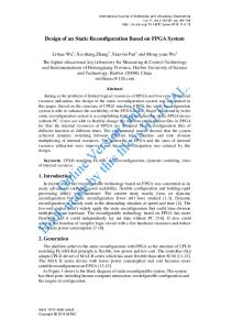
Currently, the most widely used Xilinx FPGA chips with partial reconfiguration capability are Virtex II and Virtex II Pro family. For these FPGA architectures, Xilinx has proposed two standard flows for partial reconfiguration process: Difference-based flow and Module-based flow [10]. With a Difference-based flow, the designer must manually edit a design with low-level changes. After the changes are completed, the partial bitstream, which contains information only regarding modifications, is generated and stored in a file. For the Module-based flow, the full design is partitioned into modules, some of which can be fixed while others can be reconfigurable. The reconfigurable fabric of the FPGA is partitioned into column-based rectangular regions in which the fixed and reconfigurable modules will be arranged based on specified area constrains. A bus macro can be used to maintain correct connections between the modules by spanning the boundaries of these rectangular regions. Fig. 1 shows the basic concept of this reconfiguration flow methodology. This makes the Module-based flow suitable for full automation, making it much more flexible than the Difference-based flow, particularly when it is considered for integration with high-level user applications. Therefore, this paper chooses the Module-based flow as the primary partial reconfiguration technique for the design and analyzes the partial reconfiguration bitstream generated by this flow. Consider the contents inside a partial reconfiguration bit file generated by the Module-based flow. It starts with a various length overhead, which can be automatically detected by searching the synchronous word “AA995566”.
External Data
B u s PR Module
M a c r o
PR Module Intermodule Signals
B u s M a c r o
Fixed Module
Fixed Module
Figure 1. . Design Layout with Two Reconfigurable Modules
For the following actual contents of the reconfiguration bitstream, it is described in terms of frames. In most Look Up Table (LUT) based FPGAs, configuration memory is arranged in column based vertical frames, i.e., one bit wide extending from the top edge of the device to the bottom. These frames are the smallest addressable segments of the FPGA configuration memory space; therefore, all operations must act on whole configuration frames. Even if only one byte inside one frame is changed, the full frame needs to be rewritten. Configuration memory frames do not directly map to any single piece of hardware; rather, they configure a narrow vertical slice of many physical resources. The platform used to develop the concepts in this paper is the Xilinx Virtex II Pro, which contains several configuration column types, including IOB, IOI, CLB, GCLK, BlockRAM, and BlockRAM Interconnect. Each type with a given number of frames, as described in Fig. 2 [9]. Each configuration frame has a unique 32-bit address that is composed of a Block Address (BA), a Major Address (MJA), a Minor Address (MNA), and a byte number [9]. The major address identifies a specific column within a block, and the minor address identifies a specific frame within a column. Among all these type of columns, the CLB columns program the configurable logic blocks, routing, and most interconnect resources. IOBs on the top and bottom edges of the device are also programmed by CLB configuration columns. The number of CLB configuration columns matches the number of physical CLB columns in the device. The first step in our research was to analyze the partial bitstream content. This analysis shows the size of the partial reconfiguration bit file under a suitable compression technique. Using the technique described below, the partial reconfiguration bitstream can be compressed to a size that is nearly linear in the number of resources in actual use, especially routing resources. The process is illustrated for the Xilinx Virtex II Pro series, which comprise the primary
Since configuration frames are arranged vertically, designs that span the fewest possible configuration frames achieve greater compression. To estimate the amount of compression achieved, let the number of unused frames be denoted by U on a system that uses B bits per frameAn estimate of the number of saved configuration bits, S, when a fixed region F per frame is given by: S = U × (B - F). Since B >> F, we find S to be nearly linear in terms of the product of U and B. Figure 2.
Column Level Configuration Memory Map [9]
device platform currently in use for many SoC applications involving partial reconfiguration. For each CLB column in a Virtex II Pro VP7 device, there are two columns of slices. To denote the configuration of these slices, 22 frames are utilized within the bitstream for a complete reconfiguration file. Each frame has a fixed size of 424 bytes. We first compared the bit files for a series of test circuits and determined that the logic for each CLB column, which is stored in the two LUTs of each slice, actually only occupies two of the 22 frames. In particular, the contents for the first slice column LUTs – i.e. with an even slice column number starting from ‘0’– can be found in the second frame, while those for the second slice column – i.e. with an odd slice column number starting from ‘1’– are in the third frame. IOB usage at the top and bottom edges of this CLB column are located in the first frame. The remainders of the frames are all used to describe the routing resources usage of the CLB column. Now consider the case of a partial reconfiguration bitstream file. During partial reconfiguration, consecutive frames can be written to the Frame Data Input Register (FDRI) in a single packet, since the Frame Address Register (FAR) is automatically incremented when each frame is written to configuration memory. In some cases, it is necessary to write to non-consecutive frames. In such instances, the new frame address must be explicitly written to the FAR. As always, one frame of padding data must be included at the end of every FDRI packet, and the word following each FDRI packet is interpreted as an AutoCRC value. However at the same time, for unused CLB frames, a compression technique is used in the partial reconfiguration bitstream file. Instead of writing 106 instances of the word value of ‘0’, which is a full frame length for Virtex II Pro VP7, the Multiple Frame Write Register (MFWR) is used as follows. Simply set the corresponding frame address to the FAR first, and then write two padding words to the MFWR (normally 0). Using this padding technique, the full-unused frame can be set with a total cost of just ten bytes in the bit file. Therefore, for each unused frame, the number of saved bytes is 414, for a 97.64% area savings per frame.
IV.
PROPOSED RESOURCE MANAGEMENT STRATEGY
Based on the structure features of partial reconfiguration bitstream file, a strategy is developed to achieve the highest compression rate to support the limited storage capacity and real-time transfer performance prevalent in SoC applications. This area management strategy needs to be carried out after the synthesis process of the design and before the translation, mapping, placing and routing steps. Since this strategy is dealing with the real physical resource arrangement, the logic elements are identified at very fine granularity, such as external pins, LUTs and D-flip flops etc., which the software tools can then directly translate and map with. 1.
Region Allocation: assign an area for the partial reconfiguration module, which is large enough to accommodate all the external input output signals at either top or the bottom edge of the designated area. With an FPGA model as Virtex II Pro VP7 or higher, an area with 40 pins or higher along the edge can be easily partitioned, which normally will be able to satisfy an 8-bit or even 16-bit module design.
2.
Pin Assignment: pick either top or the bottom edge and place all the external signals along the side adjacent to each other, if possible. When the assigned area contains the left or the right edge of the device, these edges may be picked as well. Placed the remainder of the pins on the other side of the edge if there is still any remaining. This step is trying to eliminate or at least minimize any unnecessary signals that will span the full height of the device, which clearly will occupy more routing resources from different frames.
3.
Column Alignment: attempt to place the entire logic element into single slice column consecutively or with only a short slice row gap, near the edge of external pins placement first. One and only one frame will be used to describe all the LUT logic contents of a full column of slices, no matter how many LUTs of the slice column are actually used as long as it is not zero. Therefore this step will minimize the number of frames used to describe the design logic as well as most of the interconnection resources.
4.
Choke-Point Elimination: if there are any logic elements with a fan out larger than 4, place the
destination elements around its side, including top and bottom of the same slice column as well as the adjacent slice column side-by-side. This normally will reduce the routing resources usage even more than simply by a mandatory placing of everything inside just one slice column. 5.
Repeat: if there are still any elements left, after finishing one column, Repeat the previous two steps. Place the rest of the logic elements into the adjacent slice column with the same principles until all or at least elements along major logic paths are finished. With an FPGA model as Virtex II Pro VP7 or higher, each slice column contains 160 or more 16-bit LUTs and the same amount of D flip-flops, which normally will be able to contain a small to middle size module design in simply one or two columns.
(a)
(b)
(c)
(d)
To summarize, the approach places the logic elements into the least slice columns as possible. The logic sequence of the elements may also need to be considered when placing along the path to achieve the highest possible optimization. V.
EXPERIMENTAL RESULTS
The hardware platform used in the experiments is Xilinx Virtex II Pro VP7 device. Module-based partial reconfiguration flow is adopted to generate the partial reconfiguration bitstream. The Xilinx ISE 6.3 is used to support the module based flow. The physical resource area management constraints are entered directly into User Constrain File (.ucf) as a text input before map and routing by the Xilinx toolsets. Four representative small case and one middle size case studies are presented which illustrated the steps and cases mentioned in the previous section. Each design was implemented as partial reconfiguration modules. Each of the four small cases has its own distinct features including parallel and cascaded LUT arrangements, dedicated physical resource usage and large fan out elements. The first design is a simple quad 4-input 16-bit LUTs design with a random combinational logic functions written in the truth table. The second design is a 9-bit shifter with cascaded logic. The third design is a 4-bit×4-bit multiplier with a block multiplier used during synthesis. And the last is again a 4-bit × 4-bit multiplier but with LUT logic only. To increase the accuracy of the comparison, all 4 modules have been defined TABLE I.
Figure 3. Design Layout
using the same amount of external signals. All these signals have been managed to place at the top edge of the partial reconfiguration region. Fig. 3 shows the optimized logic elements arrangement of all 4 designs. For the simple 4 LUT element design in Case 1, since all LUTs are in the parallel logic path with direct input from external signals and straightly feed to the output though flip flops, putting them in a single column close to the external pins is a straightforward solution. The resource arrangement is shown is Fig. 3(a). Case 2 for the shifter is shown in Fig. 3(b), since all logic elements are logically serially cascaded, from input to output, the simple single column solution is again the best choice. However, for the 4-bit×4-bit multiplier using the dedicated hardware block multiplier resource, which is circled in red in Fig. 3(c), position of the slice column needs to be balanced to minimize the routing between the path of
OPTIMIZATION RESULTS
Module name
# of LUT.
# of FF
# of block Multiplier
# of Slices
Original File Size (Byte)
Original MAX Delay (ns)
Optimized File Size (byte)
4 LUTs Shifter Block Multiplier LUT Multiplier SECDED
4 1 8 22 93
16 24 25 22 41
0 0 1 0 0
12 13 17 22 74
64K 87K 88K 96K 89K
1.371 1.377 1.346 1.367 1.355
55K 63K 66K 68K 60K
Optimized MAX Delay (ns) 1.347 1.367 1.346 1.346 1.355
Area Saving 14% 28% 25% 29% 33%
the block multiplier and the LUTs and the path of the LUTs and the external pins. This extra cost of routing also explains the decreased savings in bitstream length compared to the shifter or the LUT-based multiplier design, as listed in Table 1. For the 4-bit×4-bit LUT-based multiplier, the high fanout situation mentioned in the previous section needs to be dealt with. The carry chains, marked in brown, red, and blue in Fig. 3(d), have multiple connections to the LUT logic elements in the deep green blocks. Therefore, these carry chains are arranged around the LUT logic blocks instead of in the simple one column style to achieve the best resource area optimization. The comparative optimization results of these four case studies are listed in Table 1. The logic resource usage of each of design is also summarized in the table. Even partial reconfiguration as small as four LUT designs achieve 14% reduction saving. The most complicated design, 4-bit×4-bit LUT-based multiplier, reached almost 30% reduction rate. While the four small case studies illustrate the concept, larger and more involved designs using partial reconfiguration design should be capable of achieving higher degrees of bitstream savings using this physical resource management strategy. Results also show that the maximum delay of most of module has also been improved. To further verify our strategy, one middle-sized module, Single Error Correction Double Error Detection (SECDED) algorithm, is also implemented with the same area management as the small cases and similar pins arrangement. 74 slices have been used to implement the algorithm, which actually occupies 2 columns of slices when doing the optimization. During the optimization process, not every slice has been specifically placed because of the large number. Only the slices on the major path are constrained instead. The final result is also listed in Table 1. As suggested before, because this is a comparatively bigger module, larger bitstream savings, as of 33% is indeed achieved. Compared to the work presented in [5], which studied a similar issue at a low level with logic level optimizations, our approach achieved a higher bit reduction rate even on simpler designs. At the same time, our approach at the physical resource level can be integrated with their technique at the logic level to cascade the compression obtained achieving a multiplicative saving. VI.
CONCLUSION
In this paper, the structure of the partial reconfiguration bitstream file is carefully studied at frame level for the Xilinx
platform. Based on the thorough understanding of the bit file organization, a physical resource area management strategy is proposed to minimize the reconfiguration overhead at physical resource level at a fine granularity, which ensures such methodology being capable to be implemented into real toolsets easily and safely. The experiments show that reduction rate can be up to 30% on four representative different cases, compared to the Xilinx toolset. A higher saving rate of 33% is even achieved for the middle size module optimization. In the future works, more experiments will be conducted on more complicated test designs to optimize the approach. A genetic algorithm wrapper is also in development to make the low-level physical area management process for partial reconfiguration fully automatic. REFERENCES [1]
Compton K., Li Zhiyuan, Cooley J., Knol S., Hauck S., “Configuration relocation and defragmentation for run-time reconfigurable computing”, Very Large Scale Integration (VLSI) Systems, IEEE Transactions on, Volume: 10, Issue: 3, pp. 209 – 220, June 2002 [2] Ganesan, S.; Vemuri, R, “An integrated temporal partitioning and partial reconfiguration technique for design latency improvement”, Design, Automation and Test in Europe Conference and Exhibition 2000. Proceedings, Paris, France, 27-30 March 2000, pp 320 – 325. [3] Gericota, M.G.; Alves, G.R.; Silva, M.L.; Ferreira, J.M., “Run-time management of logic resources on reconfigurable systems”, Design, Automation and Test in Europe Conference and Exhibition, Messe Munich, Germany, 3-7 March 2003, pp. 974 – 979. [4] Hauck, S.; Zhiyuan Li; Schwabe, E., “Configuration compression for the Xilinx XC6200 FPGA”, Computer-Aided Design of Integrated Circuits and Systems, IEEE Transactions on, Volume: 18, Issue: 8, pp. 1107 – 1113, Aug. 1999. [5] Raghuraman K.P., Wang Haibo, Tragoudas S., “A novel Approach to minimize reconfiguration cost for LUT-based FPGAs”, Prodeedings of the 18th International Conference on VLSI Design (VLSID’05), Kolkata, India, January 3-7, 2005. [6] Shirazi, N.; Luk, W.; Cheung, P.Y.K , “Automating production of run-time reconfigurable designs”,. FPGAs for Custom Computing Machines, 1998. Proceedings. IEEE Symposium on, Napa Valley, CA, 15-17April 1998, pp. 147 – 156. [7] Wai-Kei Mak, Young, E.F.Y., “Temporal logic replication for dynamically reconfigurable FPGA partitioning”, Computer-Aided Design of Integrated Circuits and Systems, IEEE Transactions on, Volume: 22, Issue: 7, pp. 952 – 959, July 2003. [8] Walder, H.; Steiger, C.; Platzner, M., “Fast online task placement on FPGAs: free space partitioning and 2D-hashing” Parallel and Distributed Processing Symposium, 2003. Proceedings. International, Nice, France, 22-26 April 2003. [9] Xilinx, Inc. “Virtex-II Pro Platform FPGA User Guide”, v2.4, Aug. 2004. [10] Xilinx, Inc. “Two Flows for Partial Reconfiguration: Module Based or Difference Based”, v1.1, Nov 2003.