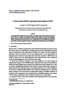
International Journal of Multimedia and Ubiquitous Engineering Vol.11, No.2 (2016), pp. 99-106 http://dx.doi.org/10.14257/ijmue.2016.11.2.12
Design of an Static Reconfiguration Based on FPGA System Li-hua Wu1, Xu-zhang Zhang1, Xiao-lei Pan1 and Meng-yuan Wu1
Abstract
L.
The higher educational key laboratory for Measuring & Control Technology and Instrumentations of Heilongjiang Province, Harbin University of Science and Technology, Harbin 150080, China
[email protected]
m Onl ad in eb eV y er th si is on fil O ei n s I ly. LL EG
A
Aiming at the problem of limited logical resources of FPGA and low rates of internal resource utilization, the design of the static reconfiguration system was introduced in this paper. Based on the structure of CPLD matching FPGA, the static reconfiguration system is able to enhance the scalability of the FPGA device. Major functionality in the static reconfiguration system is accomplishing field reconfiguration of the FPGA device without PC. Users are able to flexibly change the different configuration files in FPGA for that the internal resources of FPGA are occupied by the configuration files of different function at different times. The experimental results showed that the system achieved dynamic switching between different logic function and time division multiplexing of internal resources. The generality of FPGA and the rates of internal resource utilization were improved and the power dissipation was reduced by this design. Keywords: CPLD matching FLASH, field reconfiguration, dynamic switching, rates of internal resource
1. Introduction
Bo
ok
In recent years, the reconfigurable technology based on FPGA was concerned as its many advantages including good scalability, flexible configuration and holding rapid processing ability with hardware. The current study mostly focus on dynamic reconfiguration but static reconfiguration fewer still have studied [1-3]. Dynamic reconfiguration is mainly used in the demanding situation at speed and time [4]. The low-end market didn’t widely apply the static reconfiguration that could time division multiplexing on hardware. The reconfigurable technology based on FPGA has more flexibility and it could independently lay out data without PC [5-6]. It also could achieve the function of complex logic circuit with a few hardware resources and reduce the system power consumption [7-10].
2. Generation The platform achieves the static reconfiguration with FPGA as the structure of CPLD matching FLASH that principle is flexible, low-power and low cost. The controller chip adopts CPLD device of MAX II series which has more flexible than other SCM [11-12]. The MAX II series device with lower power consumption and cost becomes more suitable reconfiguration on FPGA [13-15]. As Figure 1 shows is the block diagram of static reconfigurable system. The system has three parts including human-computer interaction, reconfigurable configuration and the targets of configuration.
ISSN: 1975-0080 IJMUE Copyright ⓒ 2016 SERSC
International Journal of Multimedia and Ubiquitous Engineering Vol.11, No.2 (2016)
Human-computer interactive unit Manual control
LED
FLASH
m Onl ad in eb eV y er th si is on fil O ei n s I ly. LL EG
A
Reconfigurable configuration unit
L.
CPLD
FPAG
Configuration targets unit
Figure 1. The Block Diagram of Static Reconfigurable System
The functions of human-computer interactive unit are setting and display. Erasing, writing and reading are controlled by the button of manual control of human-computer interactive unit and the state of reconfiguration is displayed by LED and nixie light of human-computer interactive unit. The functions of the unit of reconfigurable configuration are storing and configuring. The FLASH chip stores the configuration files after deserializing from PC and the CPLD controller configures FPGA as the way of PS. The configuration targets unit could achieve the function of configuration files [16]. It is the unit which ultimately expresses the function of the reconfigurable platform [17].
3. The Design of CPLD Matching FLASH Structure
Bo
ok
The FPGA platform of structure based on look-up SRAM table will result in loss the configurable data after power off. So, the memory device was installed beside the FPGA in this paper. The configuration files that were stored in the FLASH device were configured to FPGA by CPLD of the static configurable platform with the way of PS. As Figure 2 shows is the circuit diagram of CPLD configure FPGA as the way of PS.
100
Copyright ⓒ 2016 SERSC
International Journal of Multimedia and Ubiquitous Engineering Vol.11, No.2 (2016)
FLASH ADDR DATA
10KΩ
CONF_DONE MSEL0 nSTATUS MSEL1 nCE DATA0 nCONFIG DCLK FPGA
nCEO
GND NC
m Onl ad in eb eV y er th si is on fil O ei n s I ly. LL EG
CONFIG_DONE nSTATUS RX TX GND DATA0 MODE nCONFIG DCLK 10KΩ CPLD
+3.3V
10KΩ
L.
DATA
A
ADDR
+3.3V
GND
Figure 2. The Circuit Diagram of CPLD Configure FPGA as the Way of PS
ok
As Figure 2 shows, there are 5 signals be used when CPLD configure FPGA as the way of PS including CONFIG_DONE(the marked signal of configuration completed), nSTATUS(the signal of configurable state), nCONFIG(the signal of configurable start), DATA0(the serial data) and DCLK(the configurable clock). The nSTATUS keeps low level and I/O pins keep high-impedance level until FPGA finish the power on reset that is a state after electrified the FPGA. The configurable period of FPGA has 3 stages including reset stage, configuration stage and initialization stage. The static configuration enters reset stage when nCONFIG or nSTATUS of FPGA is low level. The nCONFIG pin became high level from low level by controller marks the beginning of configuration stage and the ending of reset stage. The nSTATUS pin is set high level via 10KΩ pull-up resistor at the configuration stage. The data of configuration that is sent by the DATA0 pin of CPLD are latched at the rising edge of the DCLK signal. And the data of configuration are successively stored in the target device under the beats of DCLK until CONFIG_DONE become the high level. It means the finish of configuration stage and the start of initialization stage that the level of CONFIG_DONE becomes high from low. At initialization stage, the internal clock of FPGA is chosen as DCLK. The FPGA device is reconfigured when the level of nCONFIG becomes high from low and then the pin of nSTATUS isn’t occupied.
Bo
4. The Design of Serial Communication Module In the static configuration platform, the serial communication module of CPLD that makes CPLD connecting FLASH and PFGA is an important tool to configure FPGA. The function of serial communication module is receiving data and sending data to the reading and writing controller module of FLASH. For validating the receiving data, the platform has a validation feature, which feedback the receiving data to PC as the serial communication. As Figure 3 shows is the block diagram of serial communication module.
Copyright ⓒ 2016 SERSC
101
TxD
RxD
International Journal of Multimedia and Ubiquitous Engineering Vol.11, No.2 (2016)
1
1
CLK
Baud rate generation module
1 CLK_8 Band
Data
1
Data_ ready
1
m Onl ad in eb eV y er th si is on fil O ei n s I ly. LL EG
A
1
8
L.
1
Receiving data module
CLK_Band
Data 8
Sending data module
Figure 3. The Block Diagram of Serial Communication Module
As Figure 3 shows, the serial communication has 5 pins including CLK(the pin of system clock input), RxD(the pin of serial input), TxD(the pin of serial output), Data(the 8 bit pins of serial data), Data_ready(the pin of data receiving state). In the platform, the system clock is 50MHz and Data connects the reading and writing controller module of FLASH. It is difficult that the baud rate with any frequency of system clock is generated. The clock of CPLD is counted as 17.361111 which is not an integer could generate the new signal as the baud rate of 115200 when the CLK is 2MHz. In general, the hardware circuit of frequency divider is a counter which can only counter integers. The serial communication has a certain degree of tolerance to the deviation of the baud rate. In the system, the statistic is used to resolve the problems that the counter can only count integers. For example, if the clock is counted as 17.361111, the result is approached to 17.361111 through that sometimes the counter counts 17 and sometimes the counter counts 18. The static configuration platform adopts accumulator instead of counter in order to realize fractions frequency division. According that the capacities of accumulator with N bits are 2 N , the frequency of CPLD clock is determined as 2 N Hz but it is simply not the situation in reality. The accumulated value of accumulator needs conversion and formula (1) is the formula of conversion.
ok
clk 2N baud ACC
(1)
Bo
In the formula (1), clk means the input clock of the system and baud means baud rate in communication process. 2 N means the capacity of accumulator with N bits and ACC means the value of accumulator with N bits. The value of clk is 2MHz and the value of baud is 115200bps in the system. If the value of N is 10, ACC could be obtained as formula (2).
ACC
1024 2 106 ≈ 59 115200
(2)
The value of ACC is 59 in formula (2). A register with 11 bits is defined in the program with Verilog HDL and it consists of an accumulator of 10 bits behind the register and a clock of baud rate at the first bit of the register. It could generate a signal with the baud rate of 115234bps that only has 0.03% deviations compared with the baud rate of 115200bps and the method satisfied the communication requirements.
102
Copyright ⓒ 2016 SERSC
International Journal of Multimedia and Ubiquitous Engineering Vol.11, No.2 (2016)
5. The Simulation and Verification
m Onl ad in eb eV y er th si is on fil O ei n s I ly. LL EG
A
L.
The configuration file in FLASH reads successfully is a very important point in the process that is CPLD achieving static reconfiguration to FPGA. After FLASH is energized or the system is reset, the state machine in CPLD enters the reading data state for ensuring the file in FPGA changed. The valid address must stable during the reading data state until stable output data is generated at output pins of FLASH. A signal of configure module makes the reading module beginning. A start signal from configure module is generated for starting reading module when every reconfiguration and then the reading module read the files from FLASH and the files are configured to the configuration module. The reading module will check the Config_done which is a signal indicating a finish of configuration from FPGA. The reading module finishes a process of reconfiguration when the Config_done is highlevel which indicate the configuration finished. The time sequence of reading operation is generated as the way of counting by counter. The result of simulation is shown in Figure 4.
Figure 4. The Figure of Simulation Result
Bo
ok
As Figure 4 shows, the module will start reading operation and the counter will start when receiving a positive pulse at read_start. The read_finish will output a positive pulse after finishing the reading for connecting the configuration module and received the data of the configuration module. The reading operation is stopped and finishing the configuration process when receiving the positive pulse of config_done. In the reading process, address shift register is used to manage address. The value of address shift register is 0 and it will be plus one after a reading operation finished. The address of reading operation is the result of that addr_ini plus the value of address shift register. To make the operation accuracy, the address shift register is cleared before the starting of the reading operation. The design enters the verification period after finished the program with Verilog HDL. The files of function configuration that include sof format and pof format need the software of serial communication transformed to CPLD in the system. Therefore, programming files with hexadecimal as hexout format is generated with device and pin options of Quartus II. The interface of device and pin options is shown in Figure 5.
Copyright ⓒ 2016 SERSC
103
m Onl ad in eb eV y er th si is on fil O ei n s I ly. LL EG
A
L.
International Journal of Multimedia and Ubiquitous Engineering Vol.11, No.2 (2016)
Figure 5. The Interfave of Device and Pin Options
Bo
ok
The files of hexout format are written in CPLD by the software of serial communication after the files generated. CPLD store the configuration files in a designated area of configuration memory when CPLD receive the configuration files. The system is verified by the waveform generator based on reconfiguration technology and the waveform generator could generate the waveform including sine wave, square wave, triangle wave and upper oblique wave. Each configuration file of each waveform is separately written and it is stored in configuration memory by the software of serial communication. In this reconfigurable platform, the different configuration files configured in FPGA could generate corresponding waveforms. The corresponding waveforms through the digital to analog converter are verified on oscilloscope and the oscillograms are shown in Figure 6.
Figure 6. The Oscillograms of Sine Wave, Square Wave, Triangle Wave and Upper Oblique Wave
104
Copyright ⓒ 2016 SERSC
International Journal of Multimedia and Ubiquitous Engineering Vol.11, No.2 (2016)
As Figure 6 shows, the platform through manual controlled without PC for reconfiguration generates the different waveforms with the frequency of 1KHz including sine wave, square wave, triangle wave and upper oblique wave. It proved that the platform of static reconfiguration with the structure of CPLD matching FLASH could change the files in FPGA and then the FPGA could achieve different function without PC.
6. Conclusions
[1] [2]
[3]
[4]
[5] [6] [7] [8]
[9]
[10]
J. M. P. Cardoso, P. C. Diniz and M. Weinhardt, “Compiling for reconfigurable computing: A survey”, ACM Computing Surveys(CSUR), vol. 42, no. 4, (2010), pp. 13-27. K. C. Tiwari, M. K. Arora and D. Singh, “An assessment of independent component analysis for detection of military targets from hyper-spectral images”, International Journal of Applied Earth Observations and Geo-information, vol. 13, no. 05, (2011), pp. 730-740. D. Cavallo, A. Neto and A. Gerini, “Connected arrays of dipoles for broadband, wide angle scanning, dual polarized applications: a novel solution to the common mode problem”, 2010 IEEE International Symposium on Phased Array Systems and Technology, Boston, (2010), pp. 906-910. F. P. Hou and D. W. Kong, “Design of a radiator array for one-dimension wide-angle scanning phased-array antenna”, 2011 IEEE CIE International Conference on Radar, Chengdu, (2011), pp. 339-341. A. Kedar and K. S. Beenamole, “Wide beam tapered slot antenna for wide angle scanning phased array antenna”, Progress In Electromagnetics Research B, vol. 8, no. 1, (2011), pp. 235-251. Y. Yao, M. Liu and W. Chen, “Analysis and design of wideband widesan planar tapered slot antenna array”, IET Microwaves, Antenna and Propagation, vol. 4, no. 10, (2010), pp. 1632-1638. R. Bayderkhani and H. R. Hassani, “Very-low-side-lobe printed tapered arc-shaped wide-slot antenna array”, IET Microwaves, Antenna and Propagation, vol. 5, no. 10, pp. 1143-1147. J. Gu, L. L. Yang and Y. X. Yang, “The Research of Multivariable Fuzzy Neural Network Controller Based on FPGA”, Journal of Harbin University of Science and Technology, vol. 16, no. 2, (2011), pp. 44-48. C. K. Hung, R. Ikeuchi and A. Hirata, “Effects of phase difference in dipole phased-array antenna above EBG substrates on SAR”, IEEE Antennas and Wireless Propagation Letters, vol. 12, no. 1, (2013), pp. 579-582. N. H. Noordin, N. Haridas and A. O. Rayis, “Antenna array with wide angle scanning properties”, 2012 6th European Conference on Antennas and Propagation (EUCAP), Pargue, (2012), pp. 16361640. J. H. Choi and T. Itoh, “Dual-band composite right/left-handed (CRLH) phased-arrya antenna”, IEEE Antennas and Wireless Propagation Letters, vol. 11, no. 1, (2012), pp. 732-735. B. Z. Wang, S. Q. Xiao and Y. Y. Bai, “Researches on pattern reconfigurable antenna and its application in phased array Proceeding of the 2011 International Workshop on Antenna Technology, Hong Kong, (2011), pp. 46-49. X. Ding, B. Z. Wang and G. D. Ge, “A broadband VHF/UHF double-whip antenna”, IEEE Transactions on Antenna and Propagation, vol. 60, no. 2, (2012), pp. 719-724. M. S. Liang, Z. H. Zhu, L. S. Fang and Z. X. Bing, “The Design of Direct-sequence Spread Spectrum Based on FPGA”, Journal of Harbin University of Science and Technology, vol. 17, no. 6, (2012), pp. 106-109. K. Wincza and S. Gruszczynski, “Microstrip antenna arrays fed by a series-parallel slot-coupled feeding network”, IEEE Antennas and Wireless Propagation Letters, vol. 10, no. 1, (2011), pp. 991994. A. J. Kerkhoff and L. Hao, “A simplified method for reducing mutual coupling effects in low frequency radio telescope phased array”, IEEE Transactions on Antenna and Propagation, vol. 59, no. 6, (2011), pp. 1838-1845. R. J. Mailloux and S. G. Santarelli, “Mutual coupling effects and their compensation in a time-delay scanned array of irregular sub-arrays”, IEEE Antennas and Wireless Propagation Letters, vol. 12, no. 1, (2013), pp. 657-660.
ok
[11]
m Onl ad in eb eV y er th si is on fil O ei n s I ly. LL EG
References
A
L.
This thesis designs a platform of static configuration and the simulation of every module and the whole system finished suggest that the platform could flexibly change the internal files of FPGA without PC. The utilization ratio of hardware resource and the universal property of FPGA are improved as the way of time division multiplexing.
Bo
[12]
[13] [14]
[15]
[16]
[17]
Copyright ⓒ 2016 SERSC
105
Bo
ok
m Onl ad in eb eV y er th si is on fil O ei n s I ly. LL EG
A
L.
International Journal of Multimedia and Ubiquitous Engineering Vol.11, No.2 (2016)
106
Copyright ⓒ 2016 SERSC