Data Sheet
Comlinear CLC1050, CLC2050, CLC4050 ®
General Description
FEATURES n Unity gain stable n 100dB voltage gain n 550kHz unity gain bandwidth n 0.5mA supply current n 20nA input bias current n 2mV input offset voltage n 3V to 36V single supply voltage range n ±1.5V to ±18V dual supply voltage range n Input common mode voltage range includes ground n 0V to VS-1.5V output voltage swing n CLC2050: improved replacement for industry standard LM358 n CLC4050: Improved replacement for industry standard LM324 n CLC1050: Pb-free SOT23-5 n CLC2050: Pb-free SOIC-8 n CLC4050: Pb-free SOIC-14
The COMLINEAR CLC1050 (single), CLC2050 (dual), and CLC4050 (quad) are voltage feedback amplifiers that are internally frequency compensated to provide unity gain stability. At unity gain (G=1), these amplifiers offer 550kHz of bandwidth. They consume only 0.5mA of supply current over the entire power supply operating range. The CLC1050, CLC2050, and CLC4050 are specifically designed to operate from single or dual supply voltages. The COMLINEAR CLC1050, CLC2050, and CLC4050 offer a common mode voltage range that includes ground and a wide output voltage swing. The combination of low-power, high supply voltage range, and low supply current make these amplifiers well suited for many general purpose applications and as alternatives to several industry standard amplifiers on the market today.
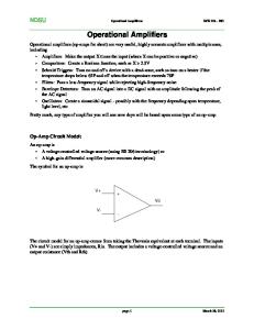
Typical Application - Voltage Controlled Oscillator (VCO)
0.05µF
APPLICATIONS n Battery Charger n Active Filters n Transducer amplifiers n General purpose controllers n General purpose instruments
R
–
100k
VCC
1/2 CLCx050
51k
–
+ R/2 50k
V+/2 51k
51k
1/2 CLCx050
Output 1
+ 100k Output 2
10k
Ordering Information Package
Pb-Free
RoHS Compliant
Operating Temperature Range
Packaging Method
CLC1050IST5X
SOT23-5
Yes
Yes
-40°C to +85°C
Reel
CLC2050ISO8X
SOIC-8
Yes
Yes
-40°C to +85°C
Reel
CLC4050ISO14X
SOIC-14
Yes
Yes
-40°C to +85°C
Reel
Moisture sensitivity level for all parts is MSL-1. Exar Corporation 48720 Kato Road, Fremont CA 94538, USA
www.exar.com Tel. +1 510 668-7000 - Fax. +1 510 668-7001
Rev 1D
Part Number
Comlinear CLC1050, CLC2050, CLC4050 Low Power, 3V to 36V, Single/Dual/Quad Amplifiers
Low Power, 3V to 36V, Single/Dual/Quad Amplifiers
Data Sheet
CLC1050 Pin Configuration
+IN
2
-IN
3
+
-
OUT
4
CLC2050 Pin Configuration
OUT1
1
8
+VS
-IN1
2
7
OUT2
+IN1
3
6
-IN2
-V S
4
5
+IN2
CLC4050 Pin Configuration
OUT1
1
14
OUT4
-IN1
2
13
-IN4
+IN1
3
12
+IN4
+VS
4
11
-VS
Pin No.
Pin Name
Description
1
+IN
Positive input
2
-VS
Negative supply
3
-IN
Negative input
4
OUT
Output
5
+VS
Positive supply
CLC2050 Pin Configuration Pin No.
Pin Name
1
OUT1
Description Output, channel 1
2
-IN1
Negative input, channel 1
3
+IN1
Positive input, channel 1
4
-VS
5
+IN2
Negative supply Positive input, channel 2
6
-IN2
Negative input, channel 2
7
OUT2
Output, channel 2
8
+VS
Positive supply
CLC4050 Pin Configuration Pin No.
Pin Name
1
OUT1
Description Output, channel 1
2
-IN1
Negative input, channel 1
3
+IN1
Positive input, channel 1
4
+VS
Positive supply
5
+IN2
Positive input, channel 2
6
-IN2
Negative input, channel 2
7
OUT2
Output, channel 2
8
OUT3
Output, channel 3
+IN2
5
10
+IN3
-IN3
Negative input, channel 3
6
9
-IN3
9
-IN2
10
+IN3
Positive input, channel 3
7
8
OUT3
11
-VS
12
+IN4
Positive input, channel 4
13
-IN4
Negative input, channel 4
14
OUT4
Output, channel 4
OUT2
Comlinear CLC1050, CLC2050, CLC4050 Low Power, 3V to 36V, Single/Dual/Quad Amplifiers
-V S
+VS
5
1
CLC1050 Pin Assignments
Negative supply
Rev 1D
©2009-2013 Exar Corporation
2/17
Rev 1D
Data Sheet
Absolute Maximum Ratings The safety of the device is not guaranteed when it is operated above the “Absolute Maximum Ratings”. The device should not be operated at these “absolute” limits. Adhere to the “Recommended Operating Conditions” for proper device function. The information contained in the Electrical Characteristics tables and Typical Performance plots reflect the operating conditions noted on the tables and plots. Supply Voltage Differential Input Voltage Input Voltage Power Dissipation (TA = 25°C) - SOIC-8 Power Dissipation (TA = 25°C) - SOIC-14
Min
Max
Unit
0
40 40 40 550 800
V V V mW mW
-0.3
Comlinear CLC1050, CLC2050, CLC4050 Low Power, 3V to 36V, Single/Dual/Quad Amplifiers
Parameter
Reliability Information Parameter
Min
Typ
Junction Temperature Storage Temperature Range Lead Temperature (Soldering, 10s) Package Thermal Resistance SOT23-5 SOIC-8 SOIC-14
-65
Max
Unit
150
°C
150 260
°C °C
221 100 88
°C/W °C/W °C/W
Notes: Package thermal resistance (qJA), JDEC standard, multi-layer test boards, still air.
Recommended Operating Conditions Parameter Operating Temperature Range Supply Voltage Range
Min -40 3 (±1.5)
Typ
Max
Unit
+85 36 (±18)
°C V
Rev 1D
©2009-2013 Exar Corporation
3/17
Rev 1D
Data Sheet
Electrical Characteristics TA = 25°C (if bold, TA = -40 to +85°C), Vs = +5V, -Vs = GND, Rf = Rg =2kΩ, RL = 2kΩ to VS/2, G = 2; unless otherwise noted. Symbol
Parameter
Conditions
Min
Typ
Max
Units
Frequency Domain Response Unity Gain Bandwidth
BWSS
-3dB Bandwidth
BWLS
Large Signal Bandwidth
G = +1, VOUT = 0.2Vpp, VS = 5V
330
kHz
G = +1, VOUT = 0.2Vpp, VS = 30V
550
kHz
G = +2, VOUT = 0.2Vpp, VS = 5V
300
kHz
G = +1, VOUT = 0.2Vpp, VS = 30V
422
kHz
G = +2, VOUT = 1Vpp, VS = 5V
107
kHz
G = +2, VOUT = 2Vpp, VS = 30V
76
kHz
VOUT = 1V step; (10% to 90%), VS = 5V
4
µs
VOUT = 2V step; (10% to 90%), VS = 30V
5.6
µs
VOUT = 0.2V step
1
%
1V step, VS = 5V
200
V/ms
4V step, VS = 30V
285
V/ms
0.015
%
> 10kHz, VS = 5V
45
nV/√Hz
> 10kHz, VS = 30V
40
nV/√Hz
Channel-to-channel, 1kHz to 20kHz
120
dB
Time Domain Response tR, tF
Rise and Fall Time
OS
Overshoot
SR
Slew Rate
Distortion/Noise Response THD
Total Harmonic Distortion
en
Input Voltage Noise
XTALK
Crosstalk
VOUT = 2Vpp, f = 1kHz, G = 20dB, CL = 100pF, VS = 30V
DC Performance VIO dVIO Ib
Input Offset Voltage (1)
Input Bias Current (1)
7 20
VCM = 0V
5
Input Offset Current (1)
VCM = 0V
PSRR
Power Supply Rejection Ratio (1)
DC, VS = 5V to 30V
Open-Loop Gain (1) Supply Current, CLC1050 (1)
IS
Supply Current, CLC2050 (1) Supply Current, CLC4050 (1)
5 7
Average Drift
IOS
AOL
2
VOUT = 1.4V, RS = 0Ω, VS = 5V to 30V
+VS = 15V, RL = ≥2kΩ, VOUT = 1V to 11V
70
mV µV/°C
100
nA
200
nA
30
nA
100
nA
100
dB
100
dB
60 85
mV
dB
80
dB
RL = ∞, VS = 30V
0.65
1.5
mA
RL = ∞, VS = 5V
0.45
1.0
mA
RL = ∞, VS = 30V
0.7
2.0
mA
RL = ∞, VS = 5V
0.5
1.2
mA
RL = ∞, VS = 30V
1.0
3.0
mA
RL = ∞, VS = 5V
0.7
1.2
mA
+VS - 1.5
V
Input Characteristics CMIR
Common Mode Input Range (1,3)
+VS = 30V
0
CMRR
Common Mode Rejection Ratio (1)
DC, VCM = 0V to (+VS - 1.5V)
60
70
dB
60
dB
26
V
Output Characteristics +VS = 30V, RL = 2kΩ Output Voltage Swing, High (1) +VS = 30V, RL = 10kΩ
©2009-2013 Exar Corporation
4/17
27 27
V 28
V V Rev 1D
Rev 1D
VOH
26
Comlinear CLC1050, CLC2050, CLC4050 Low Power, 3V to 36V, Single/Dual/Quad Amplifiers
UGBWSS
Data Sheet
Electrical Characteristics continued TA = 25°C (if bold, TA = -40 to +85°C), Vs = +5V, -Vs = GND, Rf = Rg =2kΩ, RL = 2kΩ to VS/2, G = 2; unless otherwise noted. Symbol
Parameter
Conditions
Min
Output Voltage Swing, Low (1)
+VS = 5V, RL = 10kΩ
ISOURCE
Output Current, Sourcing (1)
VIN+ = 1V, VIN- = 0V, +VS = 15V, VOUT = 2V
ISINK
Output Current, Sinking
(1)
VIN+ = 0V, VIN- = 1V, +VS = 15V, VOUT = 2V VIN+ = 0V, VIN- = 1V, +VS = 15V, VOUT = 0.2V
ISC
Short Circuit Output Current (1)
+VS = 15V
5 20
Max
Units
20
mV
30
mV
40
mA
15
mA
20 10 5 12
50 40
μA 60
mA
Notes: 1. 100% tested at 25°C. (Limits over the full temperature range are guaranteed by design.) 2. The input common mode voltage of either input signal voltage should be kept > 0.3V at 25°C. The upper end of the common-mode voltage range is +VS - 1.5V at 25°C, but either or both inputs can go to +36V without damages, independent of the magnitude of VS.
Comlinear CLC1050, CLC2050, CLC4050 Low Power, 3V to 36V, Single/Dual/Quad Amplifiers
VOL
Typ
Rev 1D
©2009-2013 Exar Corporation
5/17
Rev 1D
Data Sheet
Typical Performance Characteristics TA = 25°C, +Vs = 30V, -Vs = GND, Rf = Rg =2kΩ, RL = 2kΩ, G = 2; unless otherwise noted. Non-Inverting Frequency Response
Inverting Frequency Response
0
G=1 Rf = 0
-5
G=2
-10
G=5
-15
G = 10
-20
Normalized Gain (dB)
Normalized Gain (dB)
5 0
G = -1
-5
G = -2
-10 -15 -20
VOUT = 0.2Vpp
-25
G = -5
G = -10
VOUT = 0.2Vpp
-25
0.01
0.1
1
10
0.01
0.1
Frequency (MHz)
Frequency Response vs. CL
CL = 10nF Rs = 0Ω CL = 5nF Rs = 0Ω
-15 -20
RL = 2K -10
RL = 5K
-15 -20
-25
RL = 1K
-5
VOUT = 0.2Vpp
RL = 10K
VOUT = 0.2Vpp
-25 0.1
1
10
0.01
0.1
Frequency (MHz)
Frequency (MHz)
Frequency Response vs. VOUT
-3dB Bandwidth vs. VOUT
5
500
400
Vout = 2Vpp
-3dB Bandwidth (KHz)
Normalized Gain (dB)
0 -5 Vout = 4Vpp -10 -15
300
200
100
-20 -25 0.01
10
0
CL = 100pF Rs = 0Ω
Normalized Gain (dB)
Normalized Gain (dB)
0
0.01
1
5
CL = 1nF Rs = 0Ω
-10
10
Frequency Response vs. RL
5
-5
1
Frequency (MHz)
0 0.1
1
10
0.0
Frequency (MHz)
1.0
2.0
3.0
4.0
VOUT (VPP)
Comlinear CLC1050, CLC2050, CLC4050 Low Power, 3V to 36V, Single/Dual/Quad Amplifiers
5
Rev 1D
©2009-2013 Exar Corporation
6/17
Rev 1D
Data Sheet
Typical Performance Characteristics TA = 25°C, +Vs = 30V, -Vs = GND, Rf = Rg =2kΩ, RL = 2kΩ, G = 2; unless otherwise noted. Non-Inverting Frequency Response at VS = 5V
Inverting Frequency Response at VS = 5V
0
G=1 Rf = 0
-5
G=2
-10
G=5
-15 -20
0
Normalized Gain (dB)
Normalized Gain (dB)
5
G = 10
-5
-25
G = -2
-10
G = -5
-15 -20
VOUT = 0.2Vpp
G = -1
G = -10
VOUT = 0.2Vpp
-25
0.01
0.1
1
10
0.01
0.1
Frequency (MHz)
Frequency Response vs. CL at VS = 5V 5
Normalized Gain (dB)
Normalized Gain (dB)
-15 -20
-5
RL = 2K RL = 5K
-15 -20
-25
RL = 1K
-10
VOUT = 0.2Vpp 0.01
RL = 10K
VOUT = 0.2Vpp
-25 0.1
1
10
0.01
0.1
Frequency (MHz)
Frequency (MHz)
Frequency Response vs. VOUT at VS = 5V
-3dB Bandwidth vs. VOUT at VS = 5V
5
400 350
0
-3dB Bandwidth (KHz)
Normalized Gain (dB)
Vout = 1Vpp -5 Vout = 2Vpp -10 -15 -20
300 250 200 150 100 50
-25 0.01
10
0
CL = 5nF Rs = 0Ω
-10
1
5
CL = 100pF Rs = 0Ω
CL = 10nF Rs = 0Ω
-5
10
Frequency Response vs. RL at VS = 5V CL = 1nF Rs = 0Ω
0
1
Frequency (MHz)
0 0.1
1
10
0.0
Frequency (MHz)
0.5
1.0
1.5
2.0
VOUT (VPP)
Comlinear CLC1050, CLC2050, CLC4050 Low Power, 3V to 36V, Single/Dual/Quad Amplifiers
5
Rev 1D
©2009-2013 Exar Corporation
7/17
Rev 1D
Data Sheet
Typical Performance Characteristics - Continued TA = 25°C, +Vs = 30V, -Vs = GND, Rf = Rg =2kΩ, RL = 2kΩ, G = 2; unless otherwise noted. Small Signal Pulse Response
Large Signal Pulse Response
4.00
Output Voltage (V)
Output Voltage (V)
2.60 2.55 2.50 2.45
3.00
2.00
1.00
2.40
0.00
2.35 0
10
20
30
40
0
50
10
20
Small Signal Pulse Response at VS = 5V
40
50
Large Signal Pulse Response at VS = 5V
2.65
4.00
2.60
3.50
Output Voltage (V)
Output Voltage (V)
30
Time (us)
Time (us)
2.55 2.50 2.45 2.40
3.00 2.50 2.00 1.50
2.35
1.00 0
10
20
30
40
50
0
10
20
Time (us)
30
40
50
Time (us)
Supply Current vs. Supply Voltage
Input Voltage Range vs. Power Supply
1
15
0.9 CLC4050
0.7
Input Voltage (+/-Vdc)
Supply Current (mA)
0.8
0.6 0.5
CLC2050
0.4
CLC1050
0.3 0.2
10 NEGATIVE
POSITIVE
5
VOUT = 0.2Vpp
0.1 0 0
5
10
15
20
25
30
35
0
40
0
Supply Voltage (V)
5
10
15
Power Supply Voltage (+/-Vdc)
Comlinear CLC1050, CLC2050, CLC4050 Low Power, 3V to 36V, Single/Dual/Quad Amplifiers
5.00
2.65
Rev 1D
©2009-2013 Exar Corporation
8/17
Rev 1D
Data Sheet
Typical Performance Characteristics - Continued TA = 25°C, +Vs = 30V, -Vs = GND, Rf = Rg =2kΩ, RL = 2kΩ, G = 2; unless otherwise noted. Voltage Gain vs. Supply Voltage
Input Current vs. Temperature 20 18 RL=2K
16
90
Input Current (nA)
Voltage Gain (dB)
105
RL=20K
14 12 10
75
8 6 4
VOUT = 0.2Vpp
2
60
0 0
8
16
24
32
40
-50
-25
0
Power Supply Voltage (V)
25
50
75
100
125
Temperature (°C)
Functional Block Diagram VCC
6µA
4µA
100µA Q5 Q6
Q2 –
Q3
Cc
Q7
Q4
Q1
Rsc
Inputs
Output +
Q11 Q10 Q8
Q9
Q13 Q12
50µA
Comlinear CLC1050, CLC2050, CLC4050 Low Power, 3V to 36V, Single/Dual/Quad Amplifiers
120
Rev 1D
©2009-2013 Exar Corporation
9/17
Rev 1D
Data Sheet
Power Dissipation
Basic Operation
Power dissipation should not be a factor when operating under the stated 2k ohm load condition. However, applications with low impedance, DC coupled loads should be analyzed to ensure that maximum allowed junction temperature is not exceeded. Guidelines listed below can be used to verify that the particular application will not cause the device to operate beyond it’s intended operating range.
Figures 1, 2, and 3 illustrate typical circuit configurations for non-inverting, inverting, and unity gain topologies for dual supply applications. They show the recommended bypass capacitor values and overall closed loop gain equations. +Vs
Input
6.8μF
0.1μF
+
Output
-
RL
0.1μF Rg
Rf
6.8μF
Figure 1. Typical Non-Inverting Gain Circuit +Vs
R1 Input
Rg
Output
6.8μF -Vs
RL
Input
Pload = ((VLOAD)RMS2)/Rloadeff
G = - (Rf/Rg) For optimum input offset voltage set R1 = Rf || Rg
6.8uF
Output
-
RL 0.1uF 6.8uF -Vs
The effective load resistor (Rloadeff) will need to include the effect of the feedback network. For instance, Rloadeff in figure 3 would be calculated as: RL || (Rf + Rg)
0.1uF
+
Vsupply = VS+ - VSPower delivered to a purely resistive load is:
Rf
Figure 2. Typical Inverting Gain Circuit +Vs
PD = Psupply - Pload
Psupply = Vsupply × IRMS supply
0.1μF
In order to determine PD, the power dissipated in the load needs to be subtracted from the total power delivered by the supplies.
Supply power is calculated by the standard power equation.
6.8μF
0.1μF
+
TJunction = TAmbient + (ӨJA × PD) Where TAmbient is the temperature of the working environment.
G = 1 + (Rf/Rg)
-Vs
Maximum power levels are set by the absolute maximum junction rating of 150°C. To calculate the junction temperature, the package thermal resistance value ThetaJA (ӨJA) is used along with the total die power dissipation.
G=1
Figure 3. Unity Gain Circuit
These measurements are basic and are relatively easy to perform with standard lab equipment. For design purposes however, prior knowledge of actual signal levels and load impedance is needed to determine the dissipated power. Here, PD can be found from PD = PQuiescent + PDynamic - PLoad Quiescent power can be derived from the specified IS values along with known supply voltage, VSupply. Load power can be calculated as above with the desired signal amplitudes using:
Comlinear CLC1050, CLC2050, CLC4050 Low Power, 3V to 36V, Single/Dual/Quad Amplifiers
Application Information
Rev 1D
©2009-2013 Exar Corporation
10/17
Rev 1D
Data Sheet
(VLOAD)RMS = VPEAK / √2 ( ILOAD)RMS = ( VLOAD)RMS / Rloadeff The dynamic power is focused primarily within the output stage driving the load. This value can be calculated as:
RS (Ω)
-3dB BW (kHz)
1nF
0
485
5nF
0
390
10nF
0
260
100
0
440
Assuming the load is referenced in the middle of the power rails or Vsupply/2. Figure 4 shows the maximum safe power dissipation in the package vs. the ambient temperature for the packages available.
Maximum Power Dissipation (W)
2.5 SOIC-16
SOT23-6
1
0.5
SOT23-5
0 -40
-20
0
20
40
For a given load capacitance, adjust RS to optimize the tradeoff between settling time and bandwidth. In general, reducing RS will increase bandwidth at the expense of additional overshoot and ringing. Overdrive Recovery
2
1.5
Table 1: Recommended RS vs. CL
60
80
Ambient Temperature (°C)
An overdrive condition is defined as the point when either one of the inputs or the output exceed their specified voltage range. Overdrive recovery is the time needed for the amplifier to return to its normal or linear operating point. The recovery time varies, based on whether the input or output is overdriven and by how much the range is exceeded. The CLCx050 will typically recover in less than 30ns from an overdrive condition. Figure 6 shows the CLC1050 in an overdriven condition.
Figure 4. Maximum Power Derating
4
VIN = 1.25Vpp G=5
3.5 3
Input Voltage (V)
Increased phase delay at the output due to capacitive loading can cause ringing, peaking in the frequency response, and possible unstable behavior. Use a series resistance, RS, between the amplifier and the load to help improve stability and settling performance. Refer to Figure 5.
3 Input
2.5
2.5
2
2
1.5
1.5 Output
1
1
0.5
0.5
0
Input
+ Rf
0
-0.5
Rs CL
-0.5 0
Output
3.5
Output Voltage (V)
Driving Capacitive Loads
4
20
40
60
80
100
Time (us)
RL
Figure 6. Overdrive Recovery
Rg
Figure 5. Addition of RS for Driving Capacitive Loads
©2009-2013 Exar Corporation
Rev 1D
Table 1 provides the recommended RS for various capacitive loads. The recommended RS values result in