by Stephen A. Edwards
Retrocomputing on an FPGA Reconstructing an 80’s-Era Home Computer with Programmable Logic The author reconstructs a computer of his childhood, an Apple II+.
As a Christmas present to myself in 2007, I implemented an 1980s-era Apple II+ in VHDL to run on an Altera DE2 FPGA board. The point, aside from entertainment, was to illustrate the power (or rather, low power) of modern FPGAs. Put another way, what made Steve Jobs his first million could be a class project for the embedded systems class I teach at Columbia University. More seriously, this project demonstrates how legacy digital electronics can be preserved and integrated with modern systems. While I didn’t have an Apple II+ playing an important role in a system, many embedded systems last far longer than their technology. The space shuttle immediately comes to mind; PDP-8s can be found running some signs for San Francisco’s BART system. What is an Apple II+? The Apple II+ (Photo 1) was one of the first really successful personal computers. Designed by Steve Wozniak (“Woz”) and introduced in 1977 [1, 2, 4], it really took off in 1978 when the 140K Disk II 5.25-inch floppy drive was introduced, followed by VisiCalc, the first spreadsheet. Fairly simple even by the standards of the day, the Apple II was built around the inexpensive 8-bit 6502 processor from
Photo 1: An Apple II+
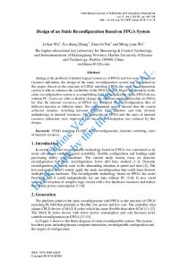
MOS Technology (it sold for $25 when an Intel 8080 sold for $179). The 6502 had an eight-bit data bus and a 64K address space. In the Apple II+, the 6502 ran at slightly above 1 MHz. Aside from the ROMs and DRAMs, the rest of the circuitry consisted of discrete LS TTL chips (Photo 2). While the first Apple IIs shipped with 4K of DRAM, this quickly grew to a standard of 48K. DRAMs, at this time, were cutting-edge technology. While they required periodic refresh and three power supplies, their six-times higher density made them worthwhile. Along with with an integrated keyboard, a rudimentary (one-bit) sound port, and a game port that could sense buttons and potentiometers (e.g., in a joystick), the main feature of an Apple II+ was its integrated video display. It generated composite (baseband) NTSC video that was usually sent through an RF modulator to appear on TV channel 3 or 4. The Apple II+ had three video modes: a 40 × 24 uppercase-only black-and-white text display, a 40 × 48 16-color low-resolution display, and a 140 × 280 6-color high-resolution display. The Apple II+ can almost be thought of as a video controller that happens to have a microprocessor connected to it. Woz started with a 14.31818 MHz master clock—exactly four times the 3.579545 MHz colorburst frequency used in NTSC video—and derived everything from it. The CPU and video alternate accesses to memory at 2 MHz. Another Woz trick: the video addresses are such that refreshing the video also suffices to refresh the DRAMs, so no additional refresh cycles are needed. Figure 1 shows the block diagram of my reconstruction. The 6502 processor on the left generates addresses and output data. The address is fed to the ROMs, an
Photo 2: The Apple II+ Motherboard. Expansion slots and analog video circuity dominate the top; the 6502 is above the six large ROM chips. The white rectangle encloses 48K of DRAM. The character ROM is at the bottom; the rest is TTL.
Figure 1: Block Diagram
Figure 2: Woz’s clock generator circuit. A 14.31818 MHz crystal drives a 4-bit shift register and a quad flip-flop to generate DRAM timing signals and the processor clocks, which in turn feed a bank of horizontal and vertical video counters. address range decoder, the peripheral slots, and to a mux that selects between processor and video system addresses for the main memory. The original Apple II+ used a tri-state data bus, but FPGA cores do not support such complex electrical structures (although they do provide tri-state I/O pins), so my reconstruction breaks the data bus into multiple segments. Most notably, I added a large mux (right side of Figure 1) that selects the source of data fed to the 6502 core, such as main memory or the ROMS. The Clock Generator Figure 2 shows the Apple’s clock generator circuit. A crystal oscillator drives the clocks on a ’195 quad shift register and a ’175 quad flip-flop. These generate clocks for the the DRAM (RAS’ and CAS’) along with the “1 MHz” processor clocks PHI0 and PHI1. A gated version of PHI0 feeds a bank of ’161s: four-bit binary counters configured to act as horizontal and vertical counters (H0–H5, VA–VC, and V0–V5) from which the video addresses are generated. This clever circuit does a lot with few parts. It is at the center of Woz’s
patent [5], which describes it and his trick of using digital signals to generate color NTSC video. Woz derived the CPU clock from the 14M clock by dividing by roughly fourteen. “Roughly” because every sixty-fifth CPU cycle (one per horizontal scan line) is stretched by two 14M clock periods to preserve the phase of the 3.58 MHz colorburst frequency. Thus, there are 65 * 14 + 2 = 912 pixel periods per line, or exactly 228 cycles of the 3.58 MHz colorburst per line. While it would be possible to write a model for each TTL part in VHDL and assemble them according to the schematic, I prefer to try to write the VHDL according to Woz’s intentions for the original circuit. This is especially true for combinational “glue” logic, which was often implemented in nonintuitive ways to save parts. Listing 1 shows my VHDL code for the clock generator. It assumes the 14 MHz clock is provided externally and consists of three main sequential processes. The first models the ’195 shift register, which either shifts or loads dependings on its own Q3 output. The second process models the ’175 quad flip-flop and the
’153 driving it, which selects between PRE PHI 0 and a combination of Q3 and PHI0 depending on the state of AX. The third sequential process models the four 4-bit binary counters. In the original circuit, these were clocked by the output of a NAND gate. Such a practice is dangerous because the output of the gate might glitch and cause unpredictable behavior, so instead I chose to clock these counters at 14 MHz and instead carefully control when they count. Figure 3 shows a timing diagram for the clock generator illustrating how it behaves at the end of a line. The COLOR DELAY N signal causes the shift register to delay RAS N et al. two extra 14M cycles, which also causes PHI0 to be stretched. HCOUNT changes on the rising edge of LDPS N, just as in the original circuit. The values taken on by the horizontal counter are a little unusual: the counter is allowed to wrap around from 7F to 00, but is then set to 40 to start the line. These 65 PHI0 periods turn into about 15.70 kHz, close to the NTSC horizontal frequency of 15.734 kHz.
61us Time CLK_14M RAS_N AX cas_n Q3
62us
63us
64us
65us
CLK_7M COLOR_REF PRE_PHI0 PHI0 LDPS_N HPE_N HCOUNT[6:0] VCOUNT[8:0] COLOR_DELAY_N
7E 0FA
7F
00 0FB
40
Figure 3: Behavior of the clock generator at the end of a line The CPU and Memory Like Woz, I didn’t create a 6502 processor from scratch. Instead, I used a 6502 core written by Peter Wendrich for his FPGA-based Commodore 64. The main challenge here was making sure it was clocked properly given the odd way the Apple II+ generates its occasionally stretched processor clock. Semiconductor memory has changed a lot since 1977. The Apple II+ used 24 4116 16-kilobit DRAM chips with 150 ns access times to provide 48 kilobytes of memory. Today, it is difficult to find memory chips this small. While it would have been nice to place all of the Apple’s memory on the FPGA I was using, it (an Altera Cyclone II 2C35) has about 59K of on-chip RAM, which is just a little too small to fit 48K of RAM plus 12K of ROMs. I chose instead to use off-chip SRAM (the DE2 has 512K) for the 48K of main memory and store the ROMs on-chip. Storing the ROMs in FPGA memory is more convenient because their contents are initialized when the FPGA is programmed. Asynchronous SRAM is much easier to interface than DRAM. The only real issue is generating an approriately timed write enable signal and making sure the tri-state data pins are only driven when the processor is writing to the RAM. The Video Generator The Apple II+ has three main video modes: a 40×24 uppercase-only text display, a 40×48 16-color “lores” graphics mode, and a 280×192 6-color
-- To generate the once-a-line hiccup: D1 pin 6 COLOR_DELAY_N