Freescale Semiconductor Technical Data
Document Number: MC34119 Rev. 3.0, 12/2006
Low Power Audio Amplifier 34119
The 34119 is a low power audio amplifier integrated circuit intended for telephone applications, such as in speakerphones. It provides differential speaker outputs to maximize output swing at low supply voltages (2.0 V minimum). Coupling capacitors to the speaker are not required. Open loop gain is 80 dB, and the closed loop gain is set with two external resistors. A Chip Disable pin permits powering down and/or muting the input signal.
LOW POWER AUDIO AMPLIFIER
Features • Wide Operating Supply Voltage Range (2.0 V to 16 V), Allows Telephone Line Powered Applications • Low Quiescent Supply Current (2.7 mA Typ) for Battery Powered Applications • Chip Disable Input to Power Down the IC • Low Power--Down Quiescent Current (65 µA Typ) • Drives a Wide Range of Speaker Loads (8.0 Ω and Up) • Output Power Exceeds 250 mW with 32 Ω Speaker • Low Total Harmonic Distortion (0.5% Typ) • Gain Adjustable from 46 dB for Voice Band • Requires Few External Components • Pb-Free Packaging Designated by Suffix Code EF
D SUFFIX EF SUFFIX (PB-FREE) 98ASB42564B 8-PIN SOICN
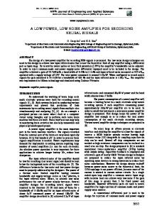
ORDERING INFORMATION Device MC34119D/R2 MCZ34119EF/R2
34199 Audio Input
VIN FC1
CC
6 5
4
V01
3 V02 8 2
FC2
1 7
CD
Chip Disable
GND
Figure 1. 34119 Simplified Application Diagram
Freescale Semiconductor, Inc. reserves the right to change the detail specifications, as may be required, to permit improvements in the design of its products.
© Freescale Semiconductor, Inc., 2007. All rights reserved.
Temperature Range (TA)
Package
-20°C to 70°C
8 SOICN
INTERNAL BLOCK DIAGRAM
INTERNAL BLOCK DIAGRAM
VCC 7
VIN 4
--
FC1 3
+
#1 4.0 k
FC2 2
50 k 125 k
5
V01
8
V02
4.0 k
-+
#2 Bias Circuit
50 k
1 CD
7 GND
Figure 2. 34119 Simplified Internal Block Diagram
34119
2
Analog Integrated Circuit Device Data Freescale Semiconductor
PIN CONNECTIONS
PIN CONNECTIONS
CD
1
8
V02
FC2
2
7
GND
FC1
3
6
VCC
VIN
4
5
V01
Figure 3. 34119 Pin Connections Table 1. 34119 Pin Definitions
Pin Number
Pin Name
Definition
1
CD
Chip Disable -- Digital input. A Logic “0” ( 30
-
MΩ
AVOL1
80
-
-
dB
AV2
-0.35
0.0
0.35
dB
GBW
-
1.5
-
MHz
POUT3
55
-
-
POUT6
240
-
-
POUT12
400
-
-
AMPLIFIERS AC Input Resistance (@ VIN) Open Loop Gain (Amplifier #1, f < 100 Hz) Closed Loop Gain (Amplifier #2, VCC = 6.0 V, f = 1.0 kHz, RL = 32Ω) Gain Bandwidth Product Output Power VCC = 3.0 V, RL = 16Ω, THD ≤ 10% VCC = 6.0 V, RL = 32Ω, THD ≤ 10% VCC = 12 V, RL = 100Ω, THD ≤ 10%% Total Harmonic Distortion (f = 1.0 kHz)
mW
THD
%
(VCC = 6.0 V, RL = 32Ω, POUT = 125 mW)
-
0.5
1.0
(VCC ≥ 3.0 V, RL = 8.0Ω, POUT = 20 mW)
-
0.5
-
(VCC ≥ 12 V, RL = 32Ω, POUT = 200 mW)
-
0.6
-
50
-
-
(C1 = 0.1 µF, C2 = 0, f = 1.0 kHz)
-
12
-
(C1 = 1.0 µF, C2 = 5.0 µF, f = 1.0 kHz)
-
52
-
-
> 70
-
Power Supply Rejection (VCC = 6.0 V, ∆VCC = 3.0 V)
PSRR
(C1 = ∞, C2 = 0.01 µF)
Differential Muting (VCC = 6.0 V, 1.0 kHz ≤ f ≤ 20 kHz, CD = 2.0 V)
GMT
dB
dB
34119
6
Analog Integrated Circuit Device Data Freescale Semiconductor
ELECTRICAL CHARACTERISTICS ELECTRICAL PERFORMANCE CURVES
ELECTRICAL PERFORMANCE CURVES
36 80
72
Phase
AVOL (dB)
108 144
60
180
Gain
40 20 0
100
1.0 k
10 k f, FREQUENCY (Hz)
100 k
Rf = 75 k, RI = 3.0 k Rf 0.1 RI
8
VO1
-#1 +
VO2
VO
#2
1.0 k 10 k f, FREQUENCY (Hz)
0 200
C1 ≥ 1.0 µF
PSRR, POWER SUPPLY REJECTION (dB)
PSRR, POWER SUPPLY REJECTION (dB)
10
1.0 k
10 k
20 k
40 30 C1 = 0
10
1.0 k
10 k
60 50
C1 = 5.0 µ F C1 = 1.0 µF
40 30
C1 = 0.1 µF
20 10 C1 = 0 0 200
1.0 k
10 k
20 k
Figure 8. Power Supply Rejection versus Frequency
C1 = 0.1 µF
0 200
C1 = 0
f, FREQUENCY (Hz) (C2= 1.0µ F)
50
20
20
20 k
Figure 5. Differential Gain versus Frequency 60
30
PSRR, POWER SUPPLY REJECTION (dB)
DIFFERENTIAL GAIN (dB)
32
0 100
C1 = 0.1 µ F
Figure 7. Power Supply Rejection versus Frequency
Rf = 150 k, RI = 6.0 k
Input
40
f, FREQUENCY (Hz) (C2= 5.0µF)
36
16
C1 ≥ 1.0 µF
50
1.0 M
Figure 4. Amplifier #1 Open Loop Gain and Phase
24
60
PSRR, POWER SUPPLY REJECTION (dB)
0 ∅, EXCESS PHASE (DEGREES)
100
20 k
f, FREQUENCY (Hz) (C2= 10 µF)
Figure 6. Power Supply Rejection versus Frequency
60 50 C1 = 5.0 µF 40 30 20 10 0 200
C1 = 1.0 µF C1 = 0.1 µF
1.0 k
10 k
20 k
f, FREQUENCY (Hz) (C2= 0)
Figure 9. Power Supply Rejection versus Frequency
34119
Analog Integrated Circuit Device Data Freescale Semiconductor
7
THD, TOTAL HARMONIC DISTORTION (%)
ELECTRICAL CHARACTERISTICS ELECTRICAL PERFORMANCE CURVES
DEVICE DISSIPATION (mW)
1000 800
VCC = 12 V VCC = 6.0 V
600 400 VCC = 3.0 V 200 0
0
30
60
90
120
10 8.0 VCC = 3.0 V, RL = 16 Ω 6.0 4.0 VCC = 16 V, RL = 32 Ω
0
100
THD, TOTAL HARMONIC DISTORTION (%)
DEVICE DISSIPATION (mW)
VCC = 12 V
800 VCC = 6.0 V
400 VCC = 3.0 V
0
100
200
300
8.0 VCC = 3.0 V, RL = 16 Ω 6.0
2.0 0 0
THD, TOTAL HARMONIC DISTORTION (%)
DEVICE DISSIPATION (mW)
800 600 400
VCC = 6.0 V VCC = 3.0 V
0 100
200
300
400
LOAD POWER (mW)
Figure 12. Device Dissipation, 32 Ω Load
VCC = 12 V, RL = 32 Ω VCC = 6.0 V, RL = 16 Ω 100 200 300 400 500 POUT , OUTPUT POWER (mW) (f= 3.0kHz,AVD = 34 dB)
Figure 14. Distortion versus Power
VCC = 12 V
VCC = 16 V
VCC = 3.0 V, RL = 8.0 Ω
VCC = 16 V, RL = 32 Ω Limit
4.0
400
1200
0
500
VCC = 6.0 V, RL = 32 Ω
Figure 11. Device Dissipation, 16 Ω Load
200
400
10
LOAD POWER (mW)
1000
300
Figure 13. Distortion versus Power
VCC = 16 V
0
200
POUT, OUTPUT POWER (mW) (f= 1.0kHz,AVD = 34 dB)
1200
200
VCC = 12 V, RL = 32 Ω
0
150
Figure 10. Device Dissipation, 8.0Ω Load
600
VCC = 6.0 V, RL = 16 Ω
2.0
LOAD POWER (mW)
1000
VCC = 6.0 V, RL = 32 Ω
VCC = 3.0 V, RL = 8.0 Ω
500
10 8.0
VCC = 3.0 V, RL = 16 Ω VCC = 3.0 V, RL = 8.0 Ω
6.0
VCC = 6.0 V, RL = 32 Ω
VCC = 16 V, RL = 32 Ω Limit
4.0
VCC = 6.0 V, RL = 16 Ω Limit
2.0
VCC = 12 V, RL = 32 Ω
0 0
100
200 300 400 POUT , OUTPUT POWER (mW) (f= 1,3.0kHz,AVD = 12 dB)
500
Figure 15. Distortion versus Power
34119
8
Analog Integrated Circuit Device Data Freescale Semiconductor
ELECTRICAL CHARACTERISTICS ELECTRICAL PERFORMANCE CURVES
500
OUTPUT 1.0 V/DIV
RL = 32 Ω
RL = 16 Ω 300 200
RL = 8.0 Ω
INPUT 80 mV/DIV
LOAD POWER (mW)
400
100 TA = 25°C--Derate at higher temperatures
0 0
2.0
4.0
6.0
8.0
10
12
14
16
20 µ s/DIV
VCC, SUPPLY VOLTAGE (V)
Figure 16. Maximum Allowable Load Power 1.5
RL = ∞
1.4
CD = 0 3.0
1.3 VCC --VOH (V)
I CC , POWER SUPPLY CURRENT (mA)
4.0
Figure 19. Large Signal Response
2.0
1.2 1.1 2.0 ≤ VCC ≤16 V
1.0
1.0 CD = VCC
0.9
0 0
2.0
4.0
6.0
8.0
10
12
14
0.8 0
16
TA = 25°C 40
VCC, SUPPLY VOLTAGE (V)
Figure 17. Power Supply Current
80
120
160
200
ILOAD, LOAD CURRENT (mA)
Figure 20. VCC-VOH @ V01, V02 versus load Current
INPUT 1.0 mV/DIV
VOL, OUTPUT LOW LEVEL (V)
OUTPUT 20 mV/DIV
1.4 1.2
TA = 25°C
VCC = 2.0 V
1.0 0.8 0.6
VCC = 3.0 V
0.4 VCC
0.2
6.0 V
0
20 µ s/DIV
0
40
80
120
160
200
ILOAD, LOAD CURRENT (mA)
Figure 18. Small Signal Response
Figure 21. VOL @ V01, V02 versus Load Current
34119
Analog Integrated Circuit Device Data Freescale Semiconductor
9
ELECTRICAL CHARACTERISTICS ELECTRICAL PERFORMANCE CURVES
AVD, DIFFERENTIAL GAIN (dB)
200
ICD , ( A)
160 120 80 40
36 32 24 16 8.0
Valid for VCD ≤ VCC 0
0
4.0
8.0
12
0 100
16
1.0 k 10 k f, FREQUENCY (Hz)
VCD, CHIP DISABLE VOLTAGE (V)
Figure 22. Input Characteristics @ CD (Pin 1)
Figure 25. Frequency Response of Figure 24 1000 pF
6 VCC
1000 pF
100 k
0.1 3.0 k
100 k
4
-#1 +
3 0.1
5 4.0 k
Input 5.0 µF
2
20 k
50 k 125 k
-+
0.05 0.05
6 VCC
Speaker 5.1 k
4.0 k
5.1 k
-#1 +
3
8
#2
4
0.1
5 4.0 k
Input
Bias Circuit
50 k
7
1
Disable
5.0 µF 2
50 k 125 k
-+
Speaker 4.0 k
50 k
GND
Differential Gain = 34 dB Frequency Response: See figure 5 Input Impedance 125 k Ω PSRR 50 dB
8
#2 Bias Circuit
1
Disable
7 GND
Figure 26. Audio Amplifier with Bandpass
Figure 23. Small Signal Response
5.1 k 5.1 k
6 VCC 4
-#1 +
3 0.1
5 4.0 k
Input 5.0 µF
2
50 k 125 k
-+
Speaker 4.0 k 8
#2
50 k
Bias Circuit
1
Disable
7
AVD, DIFFERENTIAL GAIN (dB)
75 k 0.05 0.05
36 32 24 16 8.0 0 100
1.0 k 10 k f, FREQUENCY (Hz)
20 k
GND
Figure 27. Frequency Response of Figure 26 Figure 24. Audio Amplifier with Bass Suppression
34119
10
Analog Integrated Circuit Device Data Freescale Semiconductor
ELECTRICAL CHARACTERISTICS ELECTRICAL PERFORMANCE CURVES
Rf 75 k 6 VCC (+1.0 V to +8.0 V) CI RI 0.1 3.0 k Audio Input
VIN
4
FC1
3
FC2
2
-#1 + 50 k 125 k
VO1
5
Speaker 4.0 k -+
4.0 k
Bias 1 Circuit
50 k
VO2
8
#2
CD
4700 20 k
7 VEE (--1.0 V to --8.0 V) NOTE:
If VCC and VEE are not symmetrical about ground then FC1 must be connected through a capacitor to ground as shown on the front page.
Chip Disable
20 k 10 k
VCC
VEE
Figure 28. Split Supply Operation
34119
Analog Integrated Circuit Device Data Freescale Semiconductor
11
FUNCTIONAL DESCRIPTION INTRODUCTION
FUNCTIONAL DESCRIPTION INTRODUCTION The 34119 is a low power audio amplifier capable of low voltage operation (VCC = 2.0 V minimum), such as that encountered in line-powered speakerphones. The circuit provides a differential output (VO1-VO2) to the speaker to maximize the available voltage swing at low voltages. The
differential gain is set by two external resistors. Pins FC1 and FC2 allow control of the amount of power supply and noise rejection, as well as providing alternate inputs to the amplifiers. The CD pin permits power down of the IC for muting purposes and to conserve power.
FUNCTIONAL INTERNAL BLOCK DESCRIPTION
Referring to the Internal Block Diagram on page 2, the internal configuration consists of two identical operational amplifiers. Amplifier #1 has an open loop gain of ≥80 dB (at f ≤ 100 Hz), and the closed loop gain is set by external resistor RF and RI. The amplifier is unity gain stable, and has a unity gain frequency of approximately 1.5 MHz. In order to adequately cover the telephone voice band (300 Hz to 3400 Hz), a maximum closed loop gain of 46 is recommended. Amplifier #2 is internally set to a gain of - 1.0 (0 dB). The outputs of both amplifiers are capable of sourcing and sinking a peak current of 200 mA. The outputs can typically swing to within ≈0.4 V above ground, and to within ≈1.3 V below VCC, at the maximum current. See Figures 20 and 21 for VOH and VOL curves. The output dc offset voltage (VO1 - VO2) is primarily a function of the feedback resistor (RF), and secondarily due to the amplifiers’ input offset voltages. The input offset voltage of the two amplifiers will generally be similar for a particular IC, and therefore nearly cancel each other at the outputs. Amplifier #1’s bias current, however, flows out of VIN (Pin 4) and through RF, forcing VO1 to shift negative by an amount equal to [RF ⋅ IIB]. VO2 is shifted positive an equal amount. The output offset voltage, specified in the Electrical Characteristics, is measured with the feedback resistor shown in the Typical Applications Circuit, and therefore takes into account the bias current as well as internal offset voltages of the amplifiers. The bias current is constant with respect to VCC.
FC1 AND FC2 Power supply rejection is provided by the capacitors (C1 and C2 in the Typical Applications Circuit) at FC1 and FC2. C2 is somewhat dominant at low frequencies, while C1 is dominant at high frequencies, as shown in the graphs of Figures 6 to 9. The required values of C1 and C2 depend on the conditions of each application. A line powered speakerphone, for example, will require more filtering than a circuit powered by a well regulated power supply. The amount of rejection is a function of the capacitors, and the equivalent impedance looking into FC1 and FC2 (listed in the Electrical Characteristics as RFC1 and RFC2). In addition to providing filtering, C1 and C2 also affect the turn-on time of the circuit at power-up, since the two
capacitors must charge up through the internal 50 k and 125 k. resistors. The graph of Figure 29 indicates the turn-on time upon application of VCC of +6.0 V. The turn-on time is ≈60% longer for VCC = 3.0 V, and ≈20% less for VCC = 9.0 V. Turn-off time is