Large Matrix Multiplication on a Novel Heterogeneous Parallel DSP Architecture Joar Sohl, Jian Wang, and Dake Liu Department of Electrical Engineering, Link¨oping University, 581 83 Link¨oping, Sweden ��������� �� ��� ����� �
Abstract. This paper introduces a novel master-multi-SIMD on-chip multi-core architecture for embedded signal processing. The parallel architecture and its memory subsystem are described in this paper. We evaluate the large size matrix multiplication performance on this parallel architecture and compare it with a SIMD-extended data parallel architecture. We also examine how well the new architecture scales for di«erent numbers of SIMD co-processors. The experimental results show that the ePUMA1 architecture’s memory subsystem can e«ectively hide the data access overhead. With its 8-way SIMD data path and multi-SIMD parallel execution, the ePUMA architecture improves the performance of matrix multiplication with a speedup of 45x from the conventional SIMD extension. Keywords: ePUMA, matrix multiplication, parallel DSP, SIMD, vector memory, permutation.
1 Introduction Parallel computing has been used in embedded signal processing for several decades to meet the increasing demand of computing power. Particularly, massive parallelism is of much importance for streaming DSP processors to achieve real-time processing on large volume streaming data[1]. One kind of data parallel architecture is the SIMD extension which is used in ARM’s Media Extensions[2] and PowerPC’s AltiVec[3]. It improves processing capability for streaming media applications while still o ering low power consumption. The SIMD extensions also simplify software development by providing a single tool-chain and processing core. Another parallel architecture known as VLIW[4] has also been proved to be an industrial success by TI’s DaVinci and ADI’s TigerShark. The VLIW processors take advantages of Instruction Level Parallelism (ILP) and eÆciently use the hardware resources to improve the application performance. However, both the SIMD based and the VLIW based architectures have shown their bottlenecks in today’s embedded systems. These systems are characterized by high performance and real-time requirements as well as power and cost constraints. The SIMD extensions’ drawback is due to its data access overhead for instructions such as vector load, shu�e, pack, and unpack, which becomes an obstacle to the performance enhancement [5]. The VLIW architecture has disadvantages at providing power-eÆcient and cost-e ective embedded processing[6]. Moreover, both of these two parallel architectures fail to scale to 1
ePUMA: embedded Parallel DSP processor architecture with Unique Memory Access.
Y. Dou, R. Gruber, and J. Joller (Eds.): APPT 2009, LNCS 5737, pp. 408–419, 2009. c Springer-Verlag Berlin Heidelberg 2009
Large Matrix Multiplication on a Novel Heterogeneous Parallel DSP Architecture
409
even higher performance demanding applications such as high definition video codec, baseband signal processing in communication base-stations, and radar signal processing. Recently, a new trend of master-multi-SIMD on-chip multi-core architectures has emerged in high performance parallel DSP design, for example the CELL processor from STI. The Cell architecture provides high performance processing for a wide range of applications. It has one master processor extended by eight SIMD co-processors aimed at data-intensive processing. Each co-processor is assigned a local memory and a DMA controller. The interconnection of these processors is through the Cell Element Interconnect Bus (EIB), which consists of four ring buses to provide high throughput at low cost[7]. The ePUMA project is carried out at the Computer Engineering Division of the Department of Electrical Engineering at Link¨oping University. This project aims to develop a novel master-multi-SIMD parallel embedded DSP processor for real-time high performance computing with low power consumption and low silicon cost. The goal will be achieved by maximally hiding the data access and control overhead of the parallel architecture. This project has design challenges that include a power eÆcient memory subsystem with the highest possible throughput, and a local multi-bank vector memory and address permutation design for low latency parallel vector data access. A parallel programming model and a program-friendly tool chain is another key design challenge. In this paper, we evaluate the performance of the ePUMA parallel architecture using an example of large-size matrix-matrix multiplication. Large matrix operations can be found in many data intensive computing applications. It is also a good candidate for parallel processing. The performance is evaluated on two di erent parallel architectures; a single 8-way SIMD extension, and ePUMA with di erent numbers of SIMD co-processors. The rest of this paper is organized as follows. An overview of the ePUMA mastermulti-SIMD architecture is provided in Section II. The memory subsystem is described in Section III. Section IV presents the implementations of matrix multiplication. The evaluation results are in Section V and Section VI concludes the paper.
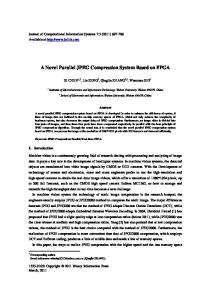
2 Overview of the ePUMA Architecture The ePUMA parallel DSP architecture is a master-multi-SIMD on-chip multi-core architecture. It consists of one master processing core, eight SIMD cores, and a memory subsystem. Each SIMD core has a local data memory and program memory. The memory subsystem includes two main memories, two ring buses, and two DMA controllers. The master core and all of the SIMD cores have access to both two buses for data and command communications. The overall architecture is illustrated in Figure 1. The master core performs scalar operations and program control, while the eight SIMD cores are assigned by the master with parallel tasks of vector processing. This parallel DSP architecture has two interfaces to two o -chip main memories. One main memory attached to Ring Bus 1 is used for streaming data storage. The second main memory on Ring Bus 2 is used for software programs and coeÆcient data. The data
410
J. Sohl, J. Wang, and D. Liu
Fig. 1. ePUMA master-multi-SIMD architecture
communications are handled by the DMA controller on each bus. Data exchange between two main memories is performed by going through the bridge module.
3 Memory Subsystem In the design of multi-core embedded processors, the memory subsystem keeps being an important component to achieve high computing performance. The memory access latency is one of the major factors that a ect performance. Moreover, the memory subsystem is the key component to reduce power consumption and silicon cost. The design of the memory subsystem determines the implementation complexity. For example, Cell EIB chooses the ring bus architecture instead of the crossbar interconnection for the purpose of getting the highest possible throughput from the wire-eÆcient ring-bus implementation with the limits on area, power and complexity costs[7]. The memory subsystem of ePUMA architecture consists of two main memories, local store unit in each SIMD core, the interconnection buses, and the DMA controller, as illustrated by the region in the dash line in Figure 1. 3.1 Interconnection Buses All the processing cores and memory modules are connected through this interconnection bus architecture, which contains two ring buses. A bridge module connects these two buses to enable data communication between them. Ring bus 1. Ring bus 1 connects the master and all SIMD cores to main memory 1 which is for streaming data storage. A DMA controller is attached to this bus for direct memory access. A DMA transaction task can be configured and triggered by either the master processor or any of the SIMD cores. Ring bus 1 uses a cross-bar bus protocol which supports multi-connections simultaneously.
Large Matrix Multiplication on a Novel Heterogeneous Parallel DSP Architecture
411
Fig. 2. Local store unit with three vector memories and two permutation tables
Ring bus 2. Ring bus 2 connects all the master and SIMD cores to main memory 2 which is prepared for software programs and coeÆcient data. Here the data communication load is not as high as in ring bus 1. To simplify implementation complexity, ring bus 2 applies a shared bus protocol, meaning that at one time only one bus master is granted the bus to perform its data transfer. 3.2 Vector Memory and Data Permutation ePUMA’s local store unit in each SIMD core consists of three vector memories and two permutation tables, as shown in Figure 2. The use of a multi-bank vector memory and data permutation can provide parallel vector data access with various addressing patterns at very short latency, usually within one cycle[8][9]. At execution time the local store unit connects two of the three vector memories to the SIMD data path for vector operands fetch. The remaining vector memory is connected to the DMA controller for data communication to the global memory. The SIMD unit works under two modes; a SIMD mode and a SIMT1 mode[1]. In SIMD mode, data are loaded to register file first and then used by the data path. While in SIMT mode, the data path can access vector memory directly. The purpose of using three vector memories is to provide a ”pingpong” bu er for simultaneously loading data and executing SIMD tasks. A switch logic is used to swap the ping-pong bu ers. Data permutation is used with the vector memories to provide conflict-free parallel access[8]. The permutation process decides each vector element’s storage position in the vector memory. This position information includes a bank number and a local address of the selected memory bank. A simple way to use a vector memory without permutation is to use a number of LSB bits from its address for bank selection, and use the rest bits as the local address. This common solution performs well for consecutive data access. For more complex SIMD or vector based high performance computing, many di erent access patterns are involved. Take matrix multiplication as an example. One matrix is accessed in row-wise order, and the other one is accessed in column-wise order. If permutation is available to provide such a column-wise vector access, the time for matrix transpose can be eliminated. This will improve the performance for matrix multiplication and other algorithms which access data that is not in row-major order. Here we give an example of using permutation to achieve conflict-free column-wise 1
SIMT stands for Single Instruction-flow Multiple Tasks [1].
412
J. Sohl, J. Wang, and D. Liu
(a) Input matrix and (b) Storage position (c) Storage position its addresses in vector memory in vector memory withoutpermutation withpermutation Fig. 3. Conflict-free vector memory access with permutation
data access, shown in Figure3. Figure 3(a) shows the source 4 4 matrix with its sequential addresses. Figure 3(b) and Figure 3(c) use a representation of �S�r� in each block to present each matrix element’s storage position in the vector memory, where S represents the bank assignment, r is the local address within the memory bank. Now we consider the access of vector �0,4,8,12�, that is, access the first column of the input matrix. Using the approach in Figure 3(b), it can be seen that all the elements are stored in memory bank 0, and a bank conflict occurs in this case. This means that four cycles are required to load this column data. When permutation is used as illustrated in Figure 3(c), the elements of the column vector reside in di erent memory banks, and no bankconflict occurs and the access latency is reduced to one cycle. The calculation of storage position �S�r� is discussed in [8] and formulated in [9]. The permutation function used in this example is shown in Equations 1 and 2. S (i) � �i � i 4� mod 4
(1)
r(i) � �i 4�
(2)
In the ePUMA local store unit, data permutation is applied on both sides of the vector memory in the form of lookup tables; the DMA controller uses one permutation table during a DMA transaction, the SIMD unit uses the other permutation table to generate data addresses for vector memory. A permutation table takes a single address either from DMA input or from SIMD load�store unit as an entry to the table, and gets an output of vector addresses for the vector memory. Each element in the address vector contains two parts, the bank number and the sub-address within that bank. These addresses are calculated by the master and the table is configured by the master processor. 3.3 Multi-task DMA Controller Each bus is allocated a DMA controller for direct memory access. A DMA transaction task can be configured either by the master core or by any of the SIMD cores. The DMA controller enables a task queue which supports multiple tasks in the queue. Thus as soon as one DMA transfer is finished, the next task can start immediately. Another useful feature of the DMA controller is the priority policy in the task queue. A task with a higher priority will be issued earlier. Simple data manipulations such as endian reordering and data width adjustment are also performed in the DMA transactions.
Large Matrix Multiplication on a Novel Heterogeneous Parallel DSP Architecture
413
4 Matrix Multiplication Implementations The main application domain for ePUMA is streaming DSP. I.e., the important algorithms that must be considered let us load a chunk of data to the vector memories, compute using a regular data access pattern, write back the results, and repeat. Algorithms that cannot be decomposed into smaller parts which have this property, i.e. those who requires irregular data access patterns and�or frequent access to main memory during the compute phases are not a priority. We do not expect the performance achieved when running these algorithms on ePUMA to deviate from the performance on other architectures in any significant way. In this section, we compare the performance of matrix multiplication of matrices with dimension 64 � 64. We chose this as our initial algorithm to be evaluated as it has very regular data access patterns and is typical for the application domain. The performance will be evaluated on two di erent architectures using three di erent software implementations. Both architectures are assumed to have an identical 8-way SIMD datapaths. The di erence between them is the complexity in memory subsystem. The first implementation is on a conventional SIMD extension data parallel architecture. The second and third implementation is on our ePUMA multi-SIMD architecture. First of all, a mathematical definition of matrix multiplication is provided in Equation 3: For A � Êm¢n � B � Ên¢ p , then C � AB � Êm¢ p , where Ci j
�
n
Ai r Br j
(3)
r 1
4.1 Architecture 1 - 8-Way SIMD Extension First we consider the case when an 8-way SIMD extension is used with a cache. For simplicity we assume that the matrices A and B are already present in the cache. We also ignore the time it takes for the output matrix C to be written back after when it is moved from the cache. However, compared to the cycles necessary for this architecture to complete the matrix multiplication it can be considered negligable. Since matrix B is in row-major order and it needs to be accessed in column-major order, we need to transpose B. Using a standard SIMDized version on 8*8 blocks this take 4810 cycles. The kernel for the matrix multiplication after B is transposed can be implementad as shown in Listing 1. While most of of the code code is quite selfexplanatory some details are worth mentioning. Using a NISO SIMD datapath[1] the computation for conv8wdw is given in Equation 4: rDest�slot �
7 i 0
Src1�i � Src2�i�
(4)
414
J. Sohl, J. Wang, and D. Liu
Similiarly, sum4dwdw is given by Equation 5: rDest�slot �
3
Src1�i � Src2�i�
(5)
i 0
To avoid lengthy code but not add overhead from jumps and managing a counter in the would be innermost loops generate is run at compile time. Similarly we use macro to avoid unneccessary repetition. Listing 1. Matrix multiplication for the 8-way SIMD extension macro CONV(REG) generate for ld ld stall conv8wdw addvs nop endgenerate endmacro
j in 0 . . 3 r0 , ( rA , r I . 0 ) r1 , ( rB , r I . 1 ) 2 REG.% j , r0 , r 1 r I , 8 �� I n c r e m e n t a d d r e s s o f f s e t s
�� rA address for matrix A rA , A �� rB address for matrix B rB , B �� rC address for matrix C rC , C i i n 0 . . 63 mul r I . 0 , i , 6 4 � WORDSIZE �� s e t o f f s e t f o r A �� r e s e t B o f f s e t set rI .1 ,0 r e p e a t 64 CONV( r 0 ) CONV( r 1 ) mul r I . 0 , i , 6 4 � WORDSIZE �� r e s e t A o f f s e t stall 2 sum4dwdw r 2 . 0 , r0 , r 1 stall 4 st m1 ( rC ) , r 4 . 0 add rC , 2 � WORDSIZE endrepeat endfor
set set set for
4.2 Architecture 2 - SIMD Co-processor with Vector Memory Using a vector memory with permutation we can implement the multiplication as shown in Figure 4. A naive implementation can be seen in Listing 2. However, since so much of the addressing overhead is removed we get a significant number of nops in the inner loop. A simple optimization by overlapping the iterations results in the code shown in Listing 3. The conv8wdw and some others instructions now use the notation � memory � (op) for operands, where op is the operation to be performed to get the address for the next
Large Matrix Multiplication on a Novel Heterogeneous Parallel DSP Architecture
415
Fig. 4. Implementation on the system with a co-processor and vector memory
operand. When we are in SIMT mode the address generator calculates these in parallel with the other instructions. The total cost of the DMA transfer is 2057 cycles. Listing 2. Matrix multiplication for ePUMA macro CONV(REG) generate for j in 0 . . 3 conv8wdw REG.% j , M1r ( · 8 ) , M2c ( · 64 � WORDSIZE � 8 ) endgenerate endmacro s e t rM1B , C f o r i i n 0 . . 63 �� s e t o f f s e t f o r A s e t rM1 , A mac rM1 , i , 6 4 � WORDSIZE �� r e s e t B o f f s e t s e t rM2 , B add r3 , B , WORDSIZE r e p e a t 64 CONV( r 0 ) CONV( r 1 ) �� r e s e t A o f f s e t s e t rM1 , A mac rM1 , i , 6 4 � WORDSIZE s e t rM2 , r 3 ·· stall 3 sum4dwdw r 2 . 0 , r0 , r 1 stall 4 st M1B( · 2 � WORDSIZE) , r 2 . 0 endrepeat endfor Listing 3. Overlapping implementation for ePUMA macro 8CONV( REG1 , REG2) generate for j in 0 . . 3 conv8wdw REG1.% j , M1r ( · 8 � WORDSIZE) , M2c ( · 64 � WORDSIZE � 8 ) endgenerate generate for j in 0 . . 2 conv8wdw REG2.% j , M1r ( · 8 � WORDSIZE) , M2c ( · 64 � WORDSIZE � 8 ) endgenerate conv8wdw REG2 . 3 , M1r ( r 6 ) , M2c ( r 7 ·· )
416
J. Sohl, J. Wang, and D. Liu
endmacro s e t rM2C , C f o r i i n 0 . . 63 set rM1 , A mac rM1 , i , 6 4 � WORDSIZE set r6 , rM1 set rM2 , B add r7 , B , WORDSIZE 8CONV( r4 , r 5 ) 8CONV( r0 , r 1 ) sum4dwdw r 2 . 0 , r4 , r 5 r e p e a t 62 8CONV( r0 , r 1 ) st M2C( · 2 � WORDSIZE) , r 2 . 0 sum4dwdw r 2 . 0 , r0 , r 1 endrepeat stall 6 st M2C( · 2 � WORDSIZE) , r 2 . 0 sum4dwdw r 2 . 0 , r0 , r 1 stall 4 st M2C( · 2 � WORDSIZE) , r 2 . 0 endfor
4.3 Architecture 2 - Overlapping DMA We can improve the performance by overlapping some DMA transactions with computation. We do not want to split matrix B into sections because the overhead per iteration for the inner loop will increase significantly. Instead we transfer matrix B in full, and then transfer each row in matrix A and the destination matrix C by themselves. This strategy lends itself well to a parallel solution by using a cyclic distribution of the rows of A and C among the SIMD processors. This is demonstrated in Figure 5 and Figure 6. In Figure 5 p � 3. We broadcast B and then send each processor one row in A. We then transfer any finished rows in C to global memory.
Fig. 5. Overlapping DMA
Large Matrix Multiplication on a Novel Heterogeneous Parallel DSP Architecture
417
In Figure 6 we see the vector memory usage. We store B in vector memory 1. Since we need to access B column-wise we use a permutation table for AGU1. Since we access A and C row-wise we do not need any permutation table for these, and we can use AGU2 and AGU3 for address generation for these memories. We do however swap vector memories 2 and 3 in the local store unit between each processed row, so that when we use one memory for calculations while the other one is used for DMA transfers.
Fig. 6. Usage of vector memories
5 Experimental Results We define the ratio R as in Equation 6: R�
Total cycles � Arithmetic instructions
(6)
The number of arithmetic instructions is defined as the number of conv8wdw and sum4dwdw instructions. For the considered implementations this value is 36864. We can then use R as a measurement for the amount of overhead for the di erent implementations. In Table 1 we find the results for when we use one core for processing for all the implementations. The ePUMA system is not that far from the ideal R value of one. We get an overhead of 19.5% with the naive DMA transactions. Being a bit more clever we get down to 15.4% by overlapping DMA transactions with computation. Using only SIMD extensions impose quite a significant overhead of 647%. The speedup of the implementations on ePUMA are quite significant, almost 6.5 when using overlapping DMA. We should also remember that we did not account for memory transfers for architecture 1, so the improvements by ePUMA should be slightly larger. Table 1. Results Architecture Arch. 1 Arch. 2 Arch. 2 - Overlapping DMA Total cycles 275342 44043
42531
R
7.469
1.195
1.154
Speedup
1.00
6.25
6.47
418
J. Sohl, J. Wang, and D. Liu
5.1 ePUMA Scalability In Table 2 we observe the relative speedup of the overlapping DMA implementation when using more than one SIMD processor. It is not quite linear; however, considering how much overhead that has already been removed it is not all that surprising that we cannot entirely hide the DMA transfers. Table 2. ePUMA scalability Processors Speedup
1
2
4
8
1.000 1.973 3.832 7.176
5.2 Permutation Tables vs Parallel Transpose In Table 3 we compare the relative execution times of using permutation tables vs performing a parallel transpose of matrix B for di erent numbers of processors. We use the values for ePUMA with permutation tables as the baseline. We can see that the added cost when not using permutation tables is 11-12%. As the transpose is �(n2 ) and the matrix multiplication is �(n3 ) we expect this value to be larger for algorithms with less computation compared to the input size. Still, avoiding an added cost of 11-12% of the total execution time is quite significant. Table 3. Using permutation tables vs parallel transpose Processors
1
2
4
8
Permutation tables 1.0000 1.0000 1.0000 1.0000 Parallel transpose 1.1147 1.1148 1.1152 1.1164
6 Conclusion Reviewing the performance increase o ered by ePUMA compared to SIMD extensions we believe that ePUMA holds great promise. Using the same number of processors as the SIMD extended architecture we increase the performance with a factor of 6.47, and by using the full 8 SIMD processor version with a factor of 45.64. While the problem at hand fits ePUMA very well it is quite reasonable to expect similar results for other algorithms with regular addressing patterns. However, we require that the data access patterns are predictable and that we will be able to load data from main memory in advance. As ePUMA is geared towards streaming DSP this is an acceptable constraint.
Acknowledgements The authors would like to thank SSF, Swedish Foundation for Strategic Research, for the support of this project.
Large Matrix Multiplication on a Novel Heterogeneous Parallel DSP Architecture
419
References 1. Liu, D.: Embedded DSP Processor Design, ch. 20. Morgen-Kaufmann, Link¨oping (2008) 2. ARM Media Extensions, �������
���������������� ���� ������ �������� 3. Tyler, J., Lent, J., Mather, A., Nauyen, H.: AltiVecT M : Bringing Vector Technology to the PowerPCT M Processor Family. In: IEEE International IPCCC 1999, February 10-12, pp. 437– 444 (1999) 4. Kumura, T., Ikekawa, M., Yosbida, M., Kuroda, I.: VLIW DSP for mobile applications. IEEE Signal Processing Magazine 19(4), 10–21 (2002) 5. Chang, H., Cho, J., Sung, W.: Performance Evaluation of an SIMD Architecture with a Multibank Vector Memory Unit. IEEE SIPS, Ban«, 71–76 (2006) 6. Weiss, M., Fettweis, G.: Dynamic Codewidth Reduction for VLIW Instruction Set Architectures in Digital Signal Processors. In: 3rd International Workshop on Image ana’ Signal Processing, pp. 517–520 (1996) 7. Ainsworth, T.W., Pinkston, T.M.: Characterizing The Cell Eib On-Chip Network. IEEE Micro 27(5), 6–14 (2007) 8. G¨ossel, M., Rebel, B., Creutzburg, R.: Memory Architecture and Parallel Access. Elsevier Science, Amsterdam (1994) ¨ 9. Lundgren, B., Odlund, A.: Expose of patterns in parallel memory access. Master thesis, Link¨oping university, LiTH-ISY-EX–07»4005-SE