FPGA Implementation of High Speed FIR Filters Using Add and Shift Method Shahnam Mirzaei, Anup Hosangadi, Ryan Kastner University Of California, Santa Barbara, CA 93106 E-mail:
[email protected],
[email protected],
[email protected] Abstract-We present a method for implementing high speed Finite Impulse Response (FIR) filters using just registered adders and hardwired shifts. We extensively use a modified common subexpression elimination algorithm to reduce the number of adders. We target our optimizations to Xilinx Virtex II devices where we compare our implementations with those produced by Xilinx CoregenTM using Distributed Arithmetic. We observe up to 50% reduction in the number of slices and up to 75% reduction in the number of LUTs for fully parallel implementations. We also observed up to 50% reduction in the total dynamic power consumption of the filters. Our designs perform significantly faster than the MAC filters, which use embedded multipliers.
most of the current generation FPGAs such as Virtex IITM have embedded multipliers to handle these multiplications, the number of these multipliers is typically limited. Furthermore, the size of these multipliers is limited to only 18 bits, which limits the precision of the computations for high speed requirements. The ideal implementation would involve a sharing of the Combinational Logic Blocks (CLBs) and these multipliers. In this paper, we present a technique that is better than conventional techniques for implementation on the CLBs. X [n] x
FPGAs are being increasingly used for a variety of computationally intensive applications, mainly in the realm of Digital Signal Processing (DSP) and communications [1-7]. Due to rapid increases in the technology, current generation of FPGAs contain a very high number of Configurable Logic Blocks (CLBs), and are becoming more feasible for implementing a wide range of applications. The high nonrecurring engineering (NRE) costs and long development time for ASICs are making FPGAs more attractive for application specific DSP solutions. DSP functions such as FIR filters and transforms are used in a number of applications such as communication and multimedia. These functions are major determinants of the performance and power consumption of the whole system. Therefore it is important to have good tools for optimizing these functions. Equation (I) represents the output of an L tap FIR filter, which is the convolution of the latest L input samples. L is the number of coefficients h(k) of the filter, and x(n) represents the input time series. k= 0, 1, ..., L-1
(I)
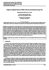
The conventional tapped delay line realization of this inner product is shown in Figure 1. This implementation translates to L multiplications and L-1 additions per sample to compute the result. This can be implemented using a single Multiply Accumulate (MAC) engine, but it would require L MAC cycles, before the next input sample can be processed. Using a parallel implementation with L MACs can speed up the performance L times. A general purpose multiplier occupies a large area on FPGAs. Since all the multiplications are with constants, the full flexibility of a general purpose multiplier is not required, and the area can be vastly reduced using techniques developed for constant multiplication. Though
1-4244-9707-X/06/$20.00 ©2006 IEEE
x
z-1
+
hL-2
x
hL-3
x
h1
x
h0 y [n]
I. INTRODUCTION
y[n] = ∑ h[k] x[n-k]
hL-1
z-1
+
z-1
...
+
z-1
z-1
+
Figure 1. A MAC FIR filter block diagram
An alternative to the above approach is Distributed Arithmetic (DA) which is a well known method to save resources. Using DA method, the filter can be implemented either in bit serial or fully parallel mode to trade bandwidth for area utilization. Assuming coefficients c[n] are known constants, equation (I) can be rewritten as follows: y[n] = ∑ c[n] · x[n]
n = 0, 1, …, N-1
(II)
Variable x[n] can be represented by: x [n] = ∑ xb [n] · 2b
b=0, 1, …, B-1 xb [n] € [0, 1]
(III)
where xb [n] is the bth bit of x[n] and B is the input width. Finally, the inner product can be rewritten as follows: y = ∑ c[n] ∑ xb [k] · 2b = c[0] (xB-1 [0]2B-1 + xB-2 [0]2B-2 + … + x0 [0]20 ) + c[1] (xB-1 [1]2B-1 + xB-2 [1]2B-2 + … + x0 [1]20 ) +… + c[N-1] (xB-1 [N-1]2B-1 + xB-2 [0]2B-2 + … + x0 [N1]20 ) = (c[0] xB-1 [0] + c[1] xB-1 [1] + … + c[N-1] xB-1 [N1])2B-1 +(c[0] xB-2 [0] + c[1] xB-2 [1] + … + c[N-1] xB-2 [N1])2B-2 +… + (c[0] x0 [0] + c[1] x0 [1] + … + c[N-1] x0 [N-1])20 = ∑ 2b ∑ c[n] · xb [k] (IV) where n=0, 1, …, N-1 and b=0, 1, …, B-1
The coefficients in most of DSP applications for the multiply accumulate operation are constants. The partial products are obtained by multiplying the coefficients ci by multiplying one bit of data xi at a time in AND operation. These partial products should be added and the result depend only on the outputs of the input shift registers. The AND functions and adders can be replaced by Look Up Tables (LUTs) that gives the partial product. This is shown in Figure 2. Input sequence is fed into the shift register at the input sample rate. The serial output is presented to the RAM based shift registers (registers are not shown in Figure for simplicity) at the bit clock rate which is n+1 times (n is number of bits in a data input sample) the sample rate. The RAM based shift register stores the data in a particular address. The outputs of registered LUTs are added and loaded to the scaling accumulator from LSB to MSB and the result which is the filter output will be accumulated over the time. For an n bit input, n+1 clock cycles are needed for a symmetrical filter to generate the output. In conventional MAC method with a limited number of MAC engines, as the filter length is increased, the system sample rate is decreased. This is not the case with serial DA architectures since the filter sample rate is decoupled from the filter length. As the filter length is increased, the throughput is maintained but more logic resources are consumed. Though the serial DA architecture is efficient by construction, its performance is limited by the fact that the next input sample can be processed only after every bit of the current input samples are processed. Each bit of the current input samples takes one clock cycle to process.
x0[i] x1[i] x2[i] x3[i]
LUT
+
x4[i] x5[i] x6[i] x7[i]
scaling accumulator