Effect of Gold Content on the Microstructural Evolution of SAC305 Solder Joints Under Isothermal Aging MIKE POWERS, JIANBIAO PAN, JULIE SILK, and PATRICK HYLAND
Au over Ni on Cu is a widely used printed circuit board (PCB) surface finish, under bump metallization (UBM), and component lead metallization. It is generally accepted that less than 3 wt.% Au in Sn-Pb solder joints inhibits formation of detrimental intermetallic compounds (IMC). However, the criti cal limit for Au content in Pb-free solder joints is not well established. Three surface-mount package platforms, one with a matte Sn surface finish and the others with Ni/Au finish, were soldered to Ni/Au-finished PCB using Sn-3.0Ag 0.5Cu (SAC305) solder, in a realistic manufacturing setting. The assembled boards were divided into three groups: one without any thermal treatment, one subjected to isothermal aging at 125°C for 30 days, and the third group aged at 125°C for 56 days. Representative solder joints were cross-sectioned and analyzed using scanning electron microscopy (SEM) and energy-disper sive x-ray spectroscopy (EDX) to investigate the evolution of the solder joint morphology as a function of Au content and isothermal aging. It was found that, if Cu is available to dissolve in the solder joint, the migration of AuSn4 from the bulk to the interface as a result of thermal aging is mitigated. Key words: Pb-free solder, isothermal aging, Ni/Au surface finish, Au content, Sn-Ag-Cu, intermetallic compound
INTRODUCTION Ni/Au over Cu is a popular finish metallization for PCB, UBM, and ball grid array/chip-scale package pads. Ni can be applied to Cu traces and pads via an electrolytic or electroless plating process and serves as a diffusion barrier layer. Au can be deposited by electrolytic, electroless, or an immersion plating process. The function of the Au layer is to protect the Ni layer from oxidation and corrosion, to enhance the wettability of solder to the surface, and in some applications, to improve wire bondability. While a thicker Au layer improves wire bondability, it can also increase the possibility of Au embrittle ment in the resulting solder joints. It is generally accepted that less than 3 wt.% Au in Sn-Pb solder joints will inhibit the formation of detrimental
IMCs.1,2 However, the critical limit for Au content in Pb-free solder joints is not well established. By now, the effect of Ni/Au on Sn-Pb solder joint reliability and the mechanism for IMC formation has been established. During the solder reflow pro cess, Au on the PCB pads (and/or on component metallizations) dissolves rapidly into the bulk mol ten solder and forms needle-like AuSn4 IMC.3 The AuSn4 IMC is distributed throughout the bulk sol der joint after reflow, and the Ni diffusion barrier reacts with Sn to form a thin Ni3Sn4 IMC at the interface. Following thermal aging at over 100°C for several hundred hours, the AuSn4 migrates to the Ni interface and forms a continuous layer of (Au,Ni)Sn4 IMC over a Ni3Sn4 IMC layer.4–6 The weak interface between (Au,Ni)Sn4 and Ni3Sn4 can lead to brittle failure.7 The driving force for the migration of AuSn4 is a reduction of Gibbs free energy by mixing.8 Au seeks Ni so that the AuSn4 becomes a Ni-saturated (Au,Ni)Sn4 compound.9
However, if the Ni barrier layer is sufficiently thin, then Cu can diffuse through the barrier to the (Au,Ni)Sn4 interface.10 In this case, the (Au,Ni)Sn4 IMC transforms to (Au,Cu,Ni)6Sn5.11 Elimination of the brittle layer of (Au,Ni)Sn4 IMC over the Ni3Sn4 layer mitigates crack propagation along the inter face. Although a thin Ni diffusion barrier layer produces this benefit, in practice Cu diffusion and oxidation can limit PCB shelf-life and hinder sol derability. The objective of this investigation is to study the morphological effect of increasing amounts of Au in SAC305 Pb-free solder joints between packaged integrated circuit (IC) components and PCBs with Au over Ni finish, and the evolution of the solder joint microstructures under isothermal aging at 125°C. An important aspect of this work is to distinguish between packaged IC platforms that employ a Ni diffusion barrier and those that do not. EXPERIMENTAL PROCEDURES Printed circuit assemblies (PCA) were manufac tured using a standard surface-mount assembly process in a realistic production environment at Jabil Circuit, San Jose, California. The test vehicle was designed as a six-layer PCB fabricated using Nelco® N4000-12 epoxy resin with an electrolytic Au over Ni finish on the Cu traces and pads. The solder paste was SAC305, 217°C melting point, type 3 with no-clean flux and a metal content of 88% by weight. The solder paste stencil was laser-cut from electro formed Ni with a thickness of 0.1 mm and a 1:1 aperture-to-pad ratio. The volume, area, and height of the solder paste on each pad were measured using a Koh Young KY-3030VAL solder paste inspection system. Solder reflow was performed in a Vitronics Soltec XPM2 belt furnace under nitrogen
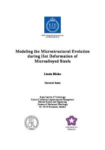
Fig. 1. Components used for PCA test vehicle.
atmosphere. The reflow temperature profile dis played a maximum heating rate of 3.2°C/s, soak time of 60 s to 120 s between 150°C and 217°C, peak temperature between 235°C and 245°C, time above liquidus of 60 s to 90 s, and maximum cooling rate of 1°C/s to 4°C/s. All of the resulting solder joints were inspected using a Phoenix Nanomex x-ray inspection system to verify joint integrity as-built. Three packaging platforms, in various sizes and configurations, were soldered to PCBs using two different Au thicknesses (thick and flash). All of the packaged IC components were daisy-chained to facilitate resistance measurements. The Au thick ness of the surface finish from random locations on the PCBs and component pads/leads was measured using a CMI XRX series x-ray fluorescence (XRF) system. The QFN platform is a quad flat no-lead packaging technology with a matte Sn finish over Cu pads (i.e., no Ni diffusion barrier). Two QFN package sizes were employed, 5 mm 9 5 mm and 6 mm 9 6 mm. The TOPS platform is a 10 mm 9 10 mm no-lead package with an open-cavity epoxy laminate construction. The pad finish on the TOPS is electrolytic Au over Ni. The FP platform is an open-cavity ceramic package with flat Kovar® (ASTM F-15 alloy) leads and an electrolytic Au over Ni finish. The FP packages have two configurations, a 6.4 mm 9 6.4 mm footprint with 12 leads and a 10.2 mm 9 9.7 mm footprint with 22 leads. Figure 1 shows photographs of the footprints for the components used in this study. The type and thickness of the metallizations on the components and boards are summarized in Table I. Due to the variation in Au thickness and solder volume at different locations on a particular board, from board to board, and on different component leads, both the average and the range of solder joint Au content were calculated. It was found that the
Table I. Metallization thickness of components and boards
QFN TOPS FP PCB
Metallization
Thickness
Matte Sn over Cu pads Ni/Au over Cu leads Ni/Au over Kovar leads Ni/Au over Cu traces
– 0.2 lm to 0.3 lm Au over 3 lm to 8 lm Ni 1 lm to 2 lm Au over 1 lm to 5 lm Ni Flash Au: 0.08 lm to 0.38 lm Au over 5 lm Ni Thick Au: 2 lm to 2.54 lm Au over 5 lm Ni
Table II. Average and range of Au content in weight percent
Flash Au board Average Range Thick Au board Average Range
QFN5
QFN6
TOPS
FPI
FPII
0.5 0.3–0.9
0.5 0.3–0.9
2.5 1.6–3.6
15.0 13.0–18.0
11.8 10.0–14.0
4.2 3.0–7.0
4.0 3.0–7.0
5.5 4.0–8.0
16.0 14.0–19.0
13.7 11.8–16.0
SAC305 solder wetted the sides and tops of Au-plated leads, which served to incrementally increase the gold content of the corresponding solder joints. The Au content in the solder joints was calculated according to Eq. (1).
wt.% Au ¼
RESULTS AND DISCUSSION The evolution of the microstructure for solder joints in this investigation is addressed in two sec tions, one based on a package substrate finish that does not have a Ni diffusion barrier (i.e., QFN) and
Au weight in component þ Au weight in PCB ; Sn-Ag-Cu weight in paste + Au weight in component + Au weight in PCB
where the Au weight in component = (area of com ponent lead) 9 (Au thickness on component lead) 9 (density of Au), the Au weight in PCB = (area of pad) 9 (Au thickness on PCB) 9 (density of Au), and Sn-Ag-Cu weight in paste = (measured solder paste volume) 9 (metal content in volume) 9 (den sity of SAC305). The average and range of Au con tent in solder joints associated with the various surface-mount package platforms are summarized in Table II. The Au content between these three package platforms on boards with thick or flash Au electroplating varies significantly. After assembly, one flash Au board and one thick Au board were randomly selected for cross-section ing and SEM/EDX analysis. This is the control group, since the PCAs did not receive any thermal aging. One group of boards was subjected to iso thermal aging at 125°C for 30 days, and another group for 56 days. After isothermal aging, one flash Au board and one thick Au board were randomly selected for cross-sectioning and SEM/EDX analy sis. The SEM used in this study was a JEOL JSM 6390 equipped with a Thermo Scientific 6733A EDX.
(1)
the other that includes a Ni barrier layer in the substrate finish. In both cases, the isothermal aging times are compared as a function of relative Au content in the solder joints. Cu/Sn-solder-Au/Ni/Cu System (