Capstone Project ENG 499
SIMUNIVERSITY SCHOOL OF SCIENCE AND TECHNOLOGY
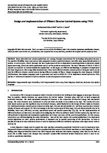
Design a voice recorder using FPGA
STUDENT: Don Lim Yuan Heng (PI NO. E0704101) SUPERVISOR: MR MAK LIN SENG PROJECT CODE: JAN2011/ENG/047
A project report submitted to SIMUniversity in partial fulfilment of requirements for the degree of Bachelor of Electronic Engineering.
Jan 2011
Capstone Project ENG 499
ABSTRACT Digital Voice Recorders have been too common and popular that is easily found and purchase at most electronic consumer market. Nowadays, they are affordable and simple/user-friendly to use which come with compact design for easy transportation, and producing high quality audio. In Modern days, Voice Recorders come with many enhancing features for examples, increase volume of speaker, recorded at a great distance, digital pitch control for distortion free sounds and built-in mic for easy record. The main objectives of this project is to design a Voice Recorder using one of the FPGA prototyping board chose on market and design together using VHDL or Verilog. The design shall be able to record a minimum of 1 minute of audio input and playback clearly through the on-board speaker or external speaker. This project has both software and hardware involve. The combination of the essential features will show how voice been record and play. The design is written in VHDL and is compiled and simulated on the Altera Cyclone II 2C20 DE 1 FPGA Development Board which was carefully chosen. This report will show these modules which design the voice recorder: RAM, controller, I2C interface and a digital audio interface. This paper also concludes on the summary, recommendations for future work and development for the project.
Capstone Project ENG 499
ACKNOWLEDGEMENT First of all, I would like to express my gratitude to my supervisor Mr Mak Lin Seng for the providing guidance, suggestion and encouragement to enable me to meet the requirement and success of this project. He has always approachable and reachable whenever I wish to seek valuable advices and comments. I am grateful to my Maintenance Supervisor, Mr Tony kie for his understanding accepting my urgent leave and time off from me continuously to focus and finish off my project during the critical time. Thanks for my colleagues who covered my duties while I am not around at work. Lastly, I wish to extend my gratitude to my family and girlfriend, Chin Yee Ting for their understanding and patience, enduring with me throughout the period.
Capstone Project ENG 499
TABLE OF CONTENTS Page ABSTRACT
2
ACKNOWLEDGEMENT
3
TABLE OF CONTENT
4
LISTS OF FIGURES
6
LIST OF TABLES
7
CHAPTER ONE INTRODUCTION
11
1.1
Background and Motivation
11
1.2
Objectives of the project
12
1.3
Project Scope
12
1.4
Layout of the Project report
13
CHAPTER TWO REVIEW OF THEORY AND PREVIOUS WORK
14
2.1 OVERVIEW OF FPGA TECHNOLOGY
14
2.1.1 The Advantages of FPGA
16
2.1.2 FPGA Application
17
2.2 OVERVIEW OF VHDL AND VERILOG
19
2.2.1 Literature Review on VHDL
19
2.2.2 Advantages of using VHDL
19
2.2.3 Literature Review on Verilog
20
2.2.4 Literature Review on VHDL and Verilog Comparison
21
2.3 OVERVIEW OF VOICE RECORDER
22
2.4 OVERVIEW OF SPEAKER
23
2.5 OVERVIEW OF MICROPHONE
24
2.6 OVERVIEW OF APPROACH AND METHOD
25
2.6.1 Proposal of Approach and method employed
25
2.6.2 Theoretical Approach
25
Capstone Project ENG 499
2.6.3 Simulation Approach
25
2.6.4 Technical Approach
26
CHAPTER 3 PROJECT PLAN
27
3.1 PROJECT MANAGEMENT
27
3.2 GANTT CHART AND SCHEDULE
27
3.3 RESOURCES REQUIRED
31
3.4 RISK ASSESSMENT
31
3.4.1 Risks identified
31
3.4.2 Migration Steps to be taken for prevention
31
3.5 PROJECT HARDWARE MANAGEMENT
33
3.5.1 Comparing of Various FPGA Board available
33
3.5.2 Selecting the most suitable board based on design requirement
35
3.5.3 Studying on the features and limitation on the chosen Board
36
3.5.4 The possible of any enhancement needed
37
3.5.5 Software Studies and Research
38
CHAPTER 4 VOICE RECORDER DESIGN IMPLEMENTATION
39
4.1 VOICE RECORDER THEORY
39
4.1.1 Speech Sampling
39
4.1.2 Sampling rate
39
4.1.3 Bit depth (quantization)
40
4.2 OVERVIEW OF THE VOICE RECORDING AND PLAYBACK
41
4.2.1 Recording process
41
4.2.2 Playing process
41
4.2.3 Explanations
42
4.3 DESIGN OF THE VOICE RECORDER 4.3.1 Design of the voice recorder controller
4.4 DESIGN OF THE I2C INTERFACE 4.4.1 I2C interface
43 43
44 44
Capstone Project ENG 499
4.4.2 The Structure of the I2C interface
46
4.4.3 Algorithm of I2C interface design
47
4.5 DIGITAL AUDIO INTERFACE DESIGN
50
4.6 THE CONTROLLER FOR A VOICE RECORDER
52
4.7 OPERATION OF ALL SYSTEM
55
4.7.1 Operation of recording
56
4.7.2 Operation of playing
57
CHAPTER 5 RESULT AND DEMONSTRATION
58
5.1 DEMONSTRATION
58
5.2 SETTING UP THE HARDWARE
58
5.3 PROGRAM THE DEVELOPMENT BOARD AS VOICE RECORDER
60
5.4 USING THE FPGA BOARD AS VOICE RECORDER
65
5.5 PROBLEMS ENCOUNTERED
69
CHAPTER 6 SUMMARY, CONCLUSION AND FUTURE WORK
72
6.1 SUMMARY
72
6.2 CONCLUSION
72
6.3 FUTURE WORK
73
CHAPTER 7 REFLECTION
74
REFERENCES
77
GLOSSARY
79
APPENDIX A: SOURCE CODE
82
A.1 RECORDER
82
A.2 ARCH CONTROL OF RECORDER
85
A.3 CONFIGURATION OF AUDIO CODEC
94
APPENDIX B: I2C INTERFACE B.1 I2C
97 98
Capstone Project ENG 499
B.2 SHIFTER OF I2C
APPENDIX C: DIGITAL INTERFACE
99
105
C.1 DIGITAL
105
C.2 ARCH OF DIGITAL
106
APPENDIX D: VOICE RECORDER PROJECT ON CYCLONE II FPGA STARTER DEVELOPMENT KIT
109
Capstone Project ENG 499
LISTS OF FIGURES
Page
Figure 2.1: Stratix 4 Series FPGA Board from Altera
14
Figure 2.2: Spartan 6 Series FPGA board from Xilinx
15
Figure 2.3: Structure of HDL modelling capability
20
Figure 2.4: examples of Digital Voice Recorder
21
Figure 2.5: Examples of Speakers
22
Figure 2.6: Examples of Microphone
23
Figure 3.1: Gantt chart
26
Figure 3.2: Altera DE1 cyclone 2 FPGA development board and accessories taken out from delivery box. 34 Figure 3.3: Altera Cyclone II 2C20 FPGA Development Board Layout and components.
35
Figure 3.4: An example of the layout of a voice recorder on the FPGA board.
36
Figure 3.5: A voice recorder block diagram concept to start with.
36
Figure 4.3 Voice Recorder Controller block diagram
42
Figure 4.4: I2C interface
43
Figure 4.4.2: The structure of I2C interface
45
Figure 4.4.3: Algorithm of I2C interface design part A
46
Figure 4.4.4: Algorithm of I2C interface design part B
47
Figure 4.4.5: Algorithm of I2C interface design part C
48
Figure 4.5.1: Block diagram of digital audio interface
49
Figure 4.5.2: Algorithm of digital audio interface
50
Figure 4.6.1: The controller for a voice recorder
51
Figure 4.6.2: Algorithm of recording process
52
Figure 4.6.3: Algorithm of playing process part A
53
Figure 4.6.4: Algorithm of playing process part B
53
Capstone Project ENG 499
Figure 4.7.1: Simple algorithm of recording
55
Figure 4.7.2: Simple algorithm of playing
56
Figure 5.2 Setting up of the hardware
58
Figure 5.3.1 Quartus II Web Edition
59
Figure 5.3.2 selection of project file
60
Figure 5.3.3 Project selection
60
Figure 5.3.4 Compilation complete
61
Figure 5.3.5 Flow summary of the compile report
62
Figure 5.3.6 Open programmer
63
Figure 5.4.1 Using FPGA as voice recorder
64
Figure 5.4.2 All switches to high
64
Figure 5.4.3 Toggle Switch 0
65
Figure 5.4.4 Toggle switch 3
65
Figure 5.4.5 Record through switch 1 and hold it
66
Figure 5.4.6 Switch 2 for playback
66
Figure 5.4.7 Green LED 0 to 7 indicate receive signal
67
Figure 5.5.1: Error on the structure of state machine
69
Figure 5.5.2: Success simulation
70
Figure 6.1: Future voice recorder enhancement with SD Card storage
72
Capstone Project ENG 499
LIST OF TABLES
page
Table 2.1: A Full simulation example of Verilog and VHDL comparison
21
Table 3.2 Project Schedule
30
Table 3.3: Comparison of Development Kit
33
Capstone Project ENG 499
CHAPTER ONE: INTRODUCTION 1.1 BACKGROUND AND MOTIVATION Methods of sound recording had undergone significant changes between first times sound was actually recorded for later playback until now. From the very first methods of recording, recording of wanted sound was difficult to capture and efficiently immediate playback. With some history of Recorder, recording was stored from cylinder to gramophone record audio disc in the 1857 and later on mic was introduced and sound was stored in various medium for examples, on magnetic tape in the 1898. Further developments on going and sound were recorded on film in the 1900, record on audio cassette in 1960s. First digital audio recorders were introduce on 1979 and recorded on Digital Audio Tape (DAT), Digital Compact Cassette (DCC) and latest technology memory use for recording is compact disc and RAM and compact cards and thumb drives. Nowadays, Voice recorders are used to take detailed notes for personal notes, interviews or lectures and any others with enhance sound capturing and clear immediate playback with a compact Voice Recording devices. However, this project enables me to create another option of technology development in another direction that includes: Implementing hardware structure and operating principle. Studies on Voice Recorder design on suitable FPGA development board platform and possible design requirement and enhancement. Studies on HDL (Hardware Development HDL (Hardware description language), VHDL (Very High speed integrated circuit Hardware Description Language) and Verilog.
Capstone Project ENG 499
1.2 OBJECTIVES OF THE PROJECT The main objective of this project is to design a Voice Recorder using VHDL or Verilog. The present project implementation shall consist of two join applications to be able to record a minimum of 1 minute of audio input and playback clearly through the on-board speaker or an external speaker. The project shall consist of Integrate knowledge which aims to contribute to the extent of development of application taken as a tool for teaching and learning, acquiring VHDL/Verilog hardware description language for communication. Purchase a development board ranging from 50-200 USD and write a VHDL/Verilog code and programmed in the on-board FPGA to realize itsfunction. By learning how to use FPGA development software toconfigure the FPGA chip for linkage of audio processing field. Thus, a better and more understanding learning from the project will be achieved.
1.3 PROJECT SCOPE The Voice Recorder is designed by selecting a most suitable FPGA prototype boards available in current market. In exchange of suitable board available from different distributors, mostly recommended and suitable board for my project in market was Altera Cyclone II 2C20 DE 1 FPGADevelopment Board.To begin with the project, first of all, we have to understand the description, the needs and the demand of the project application. These understanding constitutes of theoretical, Simulation and Technical approach and research of the technologies. The list of tasks needed to achieve the objective of this project shown below:
Literature research and review on Voice Recorder.
Familiarize with the Altera Cyclone II 2C20 DE 1 FPGA development kit hardware structure which had been selected and purchased.
Implementation of function and architecture of voice recorder on Altera Cyclone II 2C20 DE 1 FPGA development board with VHDL coding.
Testing and simulation successfully of the voice recorder system through recording and playback with the help of Quartus software.
Capstone Project ENG 499
Writing and finalise on the Final report.
1.4 LAYOUT OF THE PROJECT REPORT This report is organized into the following:
Introduction
Objective and scope of the project
Review of Theory and previous work
Overview of VHDL/Verilog, speaker, microphone
Overview of Approach and Method.
Project planning and management
Project hardware management
Overview and design of the Voice recorder
Overview of the design of I2C interface, Audio interface and controller
Result and demonstration
Summary, conclusion and future work
Reflection
Reference and glossary
Appendix of the source codes
Capstone Project ENG 499
CHAPTER TWO: REVIEW OF THEORY AND PREVIOUS WORK 2.1 Overview of FPGA Technology A Field-programmable Gate Array (FPGA) is an integrated circuit designed to be configured by the customer or designer after manufacturing—hence "fieldprogrammable". The FPGA configuration is generally specified using a hardware description language (HDL), similar to that used for an application-specific integrated circuit (ASIC) (circuit diagrams were previously used to specify the configuration, as they were for ASICs, but this is increasingly rare). FPGAs can be used to implement any logical function that an ASIC could perform. With the ability to update the functionality after shipping, partial re-configuration of the portion of the design and the low non-recurring engineering costs relative to an ASIC design (notwithstanding the generally higher unit cost); offer the advantages for many applications. FPGAs contain programmable logic components called "logic blocks", and a hierarchy of reconfigurable interconnects that allow the blocks to be "wired together"—somewhat like many (changeable) logic gates that can be inter-wired in (many) different configurations. Logic blocks can be configured to perform complex combinational functions, or merely simple logic gates like AND and XOR. In most FPGAs, the logic blocks also include memory elements, which may be simple flipflops or more complete blocks of memory. In addition to digital functions, some FPGAs have analog features. The most common analog feature is programmable slew rate and drive strength on each output pin, allowing the engineer to set slow rates on lightly loaded pins that would otherwise ring unacceptably, and to set stronger, faster rates on heavily loaded pins on highspeed channels that would otherwise run too slow. Another relatively common analog feature is differential comparators on input pins designed to be connected to differential signalling channels. A few "mixed signal FPGAs" have integrated peripheral Analog-to-Digital Converters (ADCs) and Digital-to-Analog Converters (DACs) with analog signal conditioning blocks allowing them to operate as a system-
Capstone Project ENG 499
on-a-chip. Such devices blur the line between an FPGA, which carries digital ones and zeros on its internal programmable interconnect fabric, and field-programmable analog array (FPAA), which carries analog values on its internal programmable interconnect fabric. Below shown the top products from the top 2 companies(refer to Figure 2.1 & Figure 2.2)
Figure 2.1: Stratix 4 Series FPGA Board from Altera
Capstone Project ENG 499
Figure 2.2: Spartan 6 Series FPGA board from Xilinx
2.1.1 The Advantages of FPGA Today, there are several FPGA prototypes board available in the market, the task here is to research and find out those by means of internet and listed company which are specialize in this fields. The main advantage of using an FPGA is the speed.Apart from that, it also has gain linked with any digital signal processing system with predefined as fixed relative toits sample frequency, furthermore time or temperature will not affected the process. In performance and reliability, been having the advantage of hardware parallelism, deterministic hardware committed to every task. FPGAs surpass the computing power of digital signalprocessors (DSPs) by breaking the hypothesis of chronological implementation and achieving further per clock cycle. The Control of inputs and outputs (I/O) at thehardware level of FPGAs also increase response times and dedicated functionality in order to go with applicationneeds.
Capstone Project ENG 499
i.
In market trend, FPGAs recommend a low-risk, speedy time-to-market solution that industrial designers can easily amend changes, fix bugs or create product derivatives at some point in the future. Basically, it is able to test concept and idea in hardware without long processing fabrication of a custom ASIC design. This in turn create time and cost saving for the same application.
ii.
In cost and long-term maintenance, as mention earlier ASICs needs processing fabrication which mean that large capital is needed to invest during the initial stage. In FPGA design, there are neither fabrication nor long processing assembly time needed, therefore cost in this area are saved.
2.1.2 FPGA Application Applications of FPGAs include digital signal processing, software-defined radio, aerospace and defence systems, ASIC prototyping, medical imaging, computer vision, speech recognition, cryptography, bioinformatics, computer hardware emulation, radio astronomy, metal detection and a growing range of other areas. FPGAs originally began as competitors to CPLDs and competed in a similar space, that of glue logic for PCBs. As their size, capabilities, and speed increased, they began to take over larger and larger functions to the state where some are now marketed as full systems on chips (SoC). Particularly with the introduction of dedicated multipliers into FPGA architectures in the late 1990s, applications which had traditionally been the sole reserve of DSPs began to incorporate FPGAs instead. FPGAs especially find applications in any area or algorithm that can make use of the massive parallelism offered by their architecture. One such area is code breaking, in particular brute-force attack, of cryptographic algorithms. FPGAs are increasingly used in conventional high performance computing applications where computational kernels such as FFT or Convolution are performed on the FPGA instead of a microprocessor.
Capstone Project ENG 499
The inherent parallelism of the logic resources on an FPGA allows for considerable computational throughput even at a low MHz clock rates. The flexibility of the FPGA allows for even higher performance by trading off precision and range in the number format for an increased number of parallel arithmetic units. This has driven a new type of processing called reconfigurable computing, where time intensive tasks are offloaded from software to FPGAs. The adoption of FPGAs in high performance computing is currently limited by the complexity of FPGA design compared to conventional software and the turn-around times of current design tools. Traditionally, FPGAs have been reserved for specific vertical applications where the volume of production is small. For these low-volume applications, the premium that companies pay in hardware costs per unit for a programmable chip is more affordable than the development resources spent on creating an ASIC for a low-volume application. Today, new cost and performance dynamics have broadened the range of viable applications.
Capstone Project ENG 499
2.2 OVERVIEW OF VHDL AND VERILOG 2.2.1 Literature Review on VHDL VHDL is the VHSIC Hardware Description Language. VHSIC is an abbreviation for Very High Speed Integrated Circuit.
It can describe the behaviour and structure of electronic systems, but is particularly suited as a language to describe the structure and behaviour of digital electronic hardware designs, such as ASICs and FPGAs as well as conventional digital circuits. VHDL is an international standard, regulated by the IEEE. Simulation and synthesis are the two main kinds of tools which operate on the VHDL language.
VHDL allows designs to be described using any methodology - top down, bottom up or middle out. VHDL can be used to describe hardware at the gate level or in a more abstract way. 2.2.2 Advantages of using VHDL VHDL offers several advantages to designer
Standard language – Readily available tools
Powerful and versatile description language
Multiple mechanisms to support design hierarchy
Versatile design reconfiguration support
Support for multiple levels of abstraction
Allows for various design methodologies
Provides technology independence
Describes a wide variety of digital hardware
Eases communication through standard language
Allows for better design management
Provides a flexible design language
Has given rise to derivative standards – waves, vital, Analog VHDL
Capstone Project ENG 499
2.2.3 Literature Review on Verilog Verilog HDL is a hardware description language used to design and document electronic systems. Verilog HDL allows designers to design at various levels of abstraction. It is the most widely used HDL with a user community of more than 50,000 active designers. Hardware description languages such as Verilog differ from software programming languages because they include ways of describing the propagation of time and signal dependencies (sensitivity). Verilog is case-sensitive, has a basic pre-processor (though less sophisticated than that of ANSI C/C++), and equivalent control flowkeywords (if/else, for, while, case, etc.), and compatible operator precedence. Syntactic differences include variable declaration, demarcation of procedural blocks (begin/end instead of curly braces {}), and many other minor differences. A Verilog design consists of a hierarchy of modules which communicate with other modules through a set of declared input, output, and bidirectional ports. Verilog's concept of 'wire' consists of both signal values (4-state: "1, 0, floating, undefined"), and strengths (strong, weak, etc.) This system allows abstract modelling of shared signal-lines, where multiple sources drive a common net. When a wire has multiple drivers, the wire's (readable) value is resolved by a function of the source drivers and their strengths. A subset of statements in the Verilog language is synthesizable. Verilog modules that conform to a synthesizable coding-style, known as RTL (register transfer level); can be physically realized by synthesis software. Synthesis-software algorithmically transforms the (abstract) Verilog source into netlist, a logically-equivalent description consisting only of elementary logic primitives (AND, OR, NOT, flip-flops, etc.) that are available in a specific FPGA or VLSI technology. Further manipulations to the netlist ultimately lead to a circuit fabrication blueprint (such as a photo mask set for an ASICor a bit stream file for an FPGA).
Capstone Project ENG 499
2.2.4 Literature Review on VHDL and Verilog Comparison Larger difference of about 30% in memory footprint was shown when back annotated timing had run during simulation. More of the significant result of difference is shown between VHDL and Verilog during the run times. VHDL simulation was 3 to 5 times faster than Verilog.
Table 2.1: A Full simulation example of Verilog and VHDL comparison
The figure below also has shown the structure of HDL modelling capability base on different level of behavioural of these two language abstraction.
Figure 2.3: Structure of HDL modelling capability
In general, VHDL provided a major advantage in simulation performance as well as speed for static and dynamic allocations which will be the main selection to be study and implement for this project.
Capstone Project ENG 499
2.3 OVERVIEW OF VOICE RECORDER Voice Recorder was common nowadays especially for a digital Voice Recorder type. A dictation machine is a sound recording device most commonly used to record speech for later playback or to be typed into print from the older days. In the construction of the project, components, VHDL modules are expected to be used for synchronizing with codec on the later on.
Figure 2.4: examples of Digital Voice Recorder
Capstone Project ENG 499
2.4 OVERVIEW OF SPEAKER Speaker application is to produce quality sound over a wide frequency range more effectively. An electro-acoustic transducer that converts electrical signals into sounds loud enough to be heard at a distance Nowadays, Mostly all household owning more than 1 speaker set, example home speakers with woofers, loud speaker and computer speaker. For this project, we only need any type of speaker to plug in audio line.
Figure 2.5: Examples of Speakers
Capstone Project ENG 499
2.5 OVERVIEW OF MICROPHONE A microphone is an acoustic-to-electric transducer or sensor that converts sound into an electrical signal. Microphones are used in many applications such as telephones, tape recorders, karaoke systems, hearing aids, motion picture production, live and recorded audio engineering, FRS radios, megaphones, in radio and television broadcasting and in computers for recording voice, speech recognition, VoIP, and for non-acoustic purposes such as ultrasonic checking or knock sensors. Most microphones today use electromagnetic induction (dynamic microphone), capacitance change (condenser microphone), piezoelectric generation, or light modulation to produce an electrical voltage signal from mechanical vibration.
Figure 2.6: Examples of Microphone
Capstone Project ENG 499
2.6 OVERVIEW OF APPROACH AND METHOD
2.6.1 Proposal Approach and method employed
To begin with the project, first of all, we have to understand the description, the needs and the demand of the project requirement. These understanding constitutes of theoretical, Simulation and Technical approach and research of the technologies which will be brief below. 2.6.2 Theoretical Approach Theoretical approach is one of the core elements to ensure success of this project. Initial phase includes detail researches, comparison, examination and understanding of various technologies and resources requirement. Reading up books /article on FPGA, VHDL/Verilog is also required. 2.6.3 Simulation Approach In this approach, we use the VHDL or Verilog programmes to help us design,develop and simulate a suitable FPGA prototype board platform to design to meet the essentials of the application of voice recorder. Steps required obtaining the desire results: 1. Evaluation and Comparison of FPGA/CPLD Boards to choose one as platform 2. Evaluate a suitable programmes out from HDL (Hardware Development HDL (hardware description language), VHDL (Very high speed integrated circuit Hardware Description Language) and Verilog for designing and modelling hardware
Capstone Project ENG 499
2.6.4 Technical Approach Technical Approach involved hardware fabrication of the suitable platform from the FPGA board. Performing technological of analysis results on the measured and simulated design with enhancement will further improve the recording from microphone and playback through suitable speaker. This system isconstructed by modules and components; they can be used separately to achievesimilar or different applications that required more complexity. Steps required to obtain a desired Voice recorder design are: 1. Requirement of setting up a serial connection from board and memory, microphone and speaker. 2. Find out a design tool used in order to describe pieces of hardware on VHD or Verilog. 3. Maximum and minimum of recording an audio into a memory, hooking up a microphone to a suitable audio line port. 4. To make the FPGA board to play the audio signal back over the speaker connected to its amp-out port when buttons is pushed. 5. To use a suitable protocol for connection and communication 6. To control the audio recording and playback through suitable terminal with using a standardcomputer (laptop/desktop).
Capstone Project ENG 499
Chapter 3:PROJECT PLAN 3.1 PROJECT MANAGMENT In this project, it is important to plan ahead, identified the main phases while progressing with the project. In each phase, it is also needed to identify the task required, effort for each task spent. Not forgetting to add in time spent in work and preparation during exam period. As such, I have come out with the Gantt chart to manage my time better. The Gantt chart will also show the duration of every task and overdue of schedule met.
3.2GANTT CHART AND SCHEDULE
Figure 3.1: Gantt chart
Capstone Project ENG 499
As you can see from the Gantt chart above, the Green colour bars mean the completion of tasks. The dark blue colour bars are the main tasks which had yet to touch on. The schedule planning base on Gantt chart is few weeks lagging behind due to preparation for exams and labs.
Task 1 – Project Proposal Writing and Submission Task 2 – Research for a Suitable FPGA Development Board for Designing voice Recorder was has to meet schedule. Selection of few similar FPGA Development Boards was considered. Task 3 – Research and writes a suitable VHDL/Verilog will take longer than expected, this is due to the lack of basic knowledge on VHDL and need time to digest. Task 4 – Evaluation of Design and Model Testing .Tasks have to be run concurrently. Finalizing of program and testing and simulation has to be performed concurrently too. This part took up a lot of time due studying on ways to solve problems and had the project to meet requirement. Task 5 – Preparations and compiling for final report and documentation will take up a lot of time as had foreseen that encountering quite a big mess of needs to organise, documentation and problem solving and simulation of task 4 at the same time. Task 6 - Finally, Preparation of presentation PowerPoint, demonstration and Poster will take up around 2 weeks roughly.
Capstone Project ENG 499
Date S/No.
Date Start
Finish
Days
Project Proposal Writing and Submission
5-Feb-11
7-Mar-11
30
1.1
Meet up with supervisor
12-Feb-11
12-Feb-11
1
1.2
Project research, proposal write up and review
13-Feb-11
17-Feb-11
5
1.3
Discussion on Project Proposal Draft with supervisor
20-Feb-11
20-Feb-11
1
1
Task Allocation
7-Marchth
1.4
Finalize project proposal (submission on 7 of March)
21-Feb-11
11
15
2
Voice Recorder using FPGA Technology Researches
8-Mar-11
18-Apr-11
41
Comparing of Various FPGA Boards available
8-Mar-11
14-Mar-11
7
2.1
16-Mar11(complete Select a suitable FPGA development board based on 2.2
design requirement
on 3rd-April-
15-Mar-11
11)
18
27-Mar-11 (complete on
2.3
Studying on features and limitation on chosen board
17-Mar-11
16-Apr-11)
30
28-Mar-11
18-Apr-11
20
19-Apr-11
3-Aug-11
108
Possibility for any improvement on the board to suit 2.4
design Software Studies via Program Writing with
3
Simulation
5-May10(complete Research on VHDL and Verilog - study and write 3.1
simple code to simulate
on 15-May-
19-Apr-11
11)
28
17-May11(complete 3.2
Voice Recording Design by VHDL or Verilog
6-May-11
on 8-Jun-11)
20
3.3
Exam Preparation
18-May-11
30-May-11
13
Capstone Project ENG 499
17-Jul11(complet e on 33.4 4
Finalize and Simulation Testing Evaluation of Final Design and Prototype Layout
31-May-11
Aug-11)
64
18-Jul-11
10-Oct-11
85
21-July11 (complete on
4.1
Finalize prototype (model and specification)
18-Jul-11
7-Aug-11)
15
4-Aug11(complete 4.2
Testing and simulation
22-Jul-11
on 2-Sep-11)
29
15-Aug11(complete on 23-Sep-
4.3
Final Testing with Numerical Trial run and amendment
5-Aug-11
11)
39
25-Aug11(complete 4.4 5
Recording of Output Simulation Result
16-Aug-11
on 10-Oct-11)
46
Project Report Writing and Documentation
26-Aug-11
10-Nov-11
78
5-Sep11(complete on 20-Sep-
5.1
Re-constructing and Combination of Info
26-Aug-11
11)
20
22-Sep11(complete 5.2
Drafting and Writing of Report
6-Sep-11
on 4-Oct-11)
29
Final check on report and poster (submission on 14th 5.3
Nov)
23-Sep-11
10-Nov-11
49
5.4
Exam Preparation
11-Nov-11
23-Nov-11
12
Preparation of Presentation
24-Nov-11
3-Nov-11
10
24-Nov-11
29-Nov-11
6
6
Final Preparation of Presentation PowerPoint and 6.1
Software Demonstration
Capstone Project ENG 499
6.2
Final Preparation (Presentation on 3rd Dec)
30-Nov-11
3-Dec-11
4
Table 3.2 Project Schedule
From Table 3.2, show the actual planning dates for different tasks and the overdue dates of completion. Overdue were mostly because of many obstacles for examples, face of problems while doing the project, studying for other courses, preparation for exams, work and personal life commitments.
3.3RESOURCE REQUIRED
Suitable FPGA Development Board
Microphone
External speaker
Laptop for presentation
VHDL and Verilog software
Communication tools for communication of application
3.4 RISK ASSESSMENT Risk assessment is done in order to plan beforehand the precaution measures to be taken off. 3.4.1 Risks identified:
Higher cost spendthrift
Overcomplicating the design process
Time availability of initial and full production of the project
Manufacturing risk in term of board burn or mal-function
Strength of manufacturer (Student)
Capabilities of the application memory limitation for recording
3.4.2 Migration Steps to be taken for prevention:
Careful selection of FPGA board base on specification before implementation
Capstone Project ENG 499
Mastering of VHDL and Verilog programming
Keen to learn and take extra measures
Self-discipline obeying and follow scheduled tasks from Gantt chart strictly.
Strong Investment in design productivity
Set up dedication
Redesign logic as a synchronous design
Careful timing analysis of new design with available tools
Memory size for recording limitation
Clock speed
Connectors
Analog Interface
Support and Resources
Capstone Project ENG 499
3.5PROJECT HARDWARE MANAGMENT 3.5.1 Comparing of Various FPGA Board available
Comparison
SMA
Clock
Memory
Connector
ADC
Price
Availability
/DAC
(USD)
and Capability
Xilinx
Spartan 3A
Yes
50 MHz
4 Mbit
2 channel
$199
Fastest in
crystal
Platform
speed. More
oscillator on-
Flash
logic,
board
PROM,
memory,
2-16
Clock, I/O.
optional user-
Mbit SPI
Embedded
installed clock
Flash
hard IP
Devices
resources.
Open slot for
More users friendly Spartan 3E
Yes
50 MHz
4-Mbyes
2 channel
$159
Similar to 3A
crystal clock
but had
oscillator
discontinued [37].
Altera
Cyclone II
Yes
Oscillator 50,
8-Mbyte
WM8731
27, 24 MHz
SDRAM,
audio
than Xilinx
clock signal
512-
CODEC
board in
driven to
Kbyte
of 2
performance
FPGA
SRAM,
channels
but had better
External clock input
$269
A bit slower
4-Mbytes
memory and
flash
record/playba
Connector to FPGA clock pin Table 3.3: Comparison of Development Kit
ck codec.
Capstone Project ENG 499
Xilinx and Altera are the current FPGA market leaders and long-time industry rivals. Together, they control over 80 percentage of the market, with Xilinx alone representing over 50 percentages. Both Xilinx and Altera provide free Windows and Linux design software. The following table shows the comparison of the development kit in the project after several facts from recommendation from forum and cost consideration from many boards and series. We chose Cyclone FPGA series from Altera which are built for low-power, cost sensitive design needs and able to get faster at market. The development board Cyclone II provides a Wolfson WM8731high-quality, 24-bit, sigma-delta audio encoder/decoder (CODEC) for applications such as MP3 players and recorders, PDAs, smart phones, and voice recorders. As from Xilinx, the Spartan-3A and 3E DSP Starter Kit is the ideal hardware platform to evaluate Xilinx FPGAs in a wide range of Video and Imaging applications. After much comparison, Cyclone 2 Starter kit is chosen because of extra space of memory and available of 24-bit WM8731 CODEC which is more suitable for this project in term of recording and playback of audio and sound. To move on, too many FPGA board associate distributors and vendor to ask for enquiries. Enquiry of the selected board and recommended suitable FPGA boards available, budget cost, base project requirement etc. in exchange of emails and calls from different distributors. Below are the Various FPGA boards recommended and available in Local country, Singapore. o Altera starter kit cyclone 3 FPGA Evaluation board o Altera DE1 cyclone 2 FPGA development board o Lattice MachX02 Control Evaluation Board
Capstone Project ENG 499
3.5.2 Selecting the most suitable Board based on design requirement
In exchange of suitable board available from different distributors, mostly recommended and suitable board for my project in market was ―Altera Cyclone II 2C20 DE 1 FPGA Development Board‖. Interest and Quotation of the DE1 board was requested from the element 14 Singapore sale company. Reply of the Quotation and discount was given then. After much consideration as the price was a bit over the limit of the budget (339.79 SGD after discount), the spec of the board is attractive and suitable. Order form was submitted and the board was delivered after 1 month and received on 15th of May 2011. Below show the components and layout of the board and accessories.
Figure 3.2: Altera DE1 cyclone 2 FPGA development board and accessories taken out from delivery box.
Capstone Project ENG 499
Below Figure 3.3 show the components and layout of the board.
Figure 3.3: Altera Cyclone II 2C20 FPGADevelopment Board Layout and components.
3.5.3 Studying on the features and limitation on the chosen Board The Altera® DE1 Development is suitable for a wide exercise from simple tasksthat fundamental concept to advanced design. DE1 consists of Line in/Line out microphone and speaker jacks for Audio demonstration most importantly, also has micro SD card socket which can use it for voice storage purpose. Testing was experimented by setting toggle switch SW9 to UP position connecting to an audio player to line in connector on the board. The headset produces expected record sound playing on the audio sound. Reformat of the whole SD card is required to erase the entire flash memory due to the limitation of software and flash memory tolerates only a limited number of erasures.
Capstone Project ENG 499
3.5.4 The possibilities of any enhancement needed
The development board provides a Wolfson WM8731high-quality, 24-bit, And use of Sigma-delta audio encoder/decoder (CODEC) for applications such as voice recorders. Below is the prototype example of the product.
Figure 3.4: An example of the layout of a voice recorder on the FPGA board.
Capstone Project ENG 499
Figure 3.5: A voice recorder block diagram concept to start with.
The possible enhancement will be modify the recorder module to implement basic record and playback functionality through incrementing the memory address after each write. Keep track of the highest memory address that's written. Fill up the possible memory on the SD Card to maximize the sound quality and recording time over the project requirement limit.
3.5.5 Software Studies and Research
Had download few HDL simulators and most frequent use of the free download of Xilinx ISEweb pack design software as it gives a slow process simulation which actually good for learning stage of beginner. Experiment by attaching my FPGA board to my desktop CPU via PCI bus on programme simulation. Besides that, I am currently reading on ―VHDL, Programming by Example by Douglas L.Perry – Fourth Edition‖ to understand the IEEE. Simulation and synthesis currently still on the learning and trying side. As you can see from the Gantt chart above, the Green colour bars mean the completion of tasks. The dark blue colour bars are the main tasks which had yet to touch on. The schedule planning base on Gantt chart is few weeks lagging behind due to preparation for exams and labs.
Capstone Project ENG 499
Chapter 4: VOICE RECORDER DESIGN IMPLEMENTATION 4.1 VOICE RECORDER THEORY
4.1.1 Speech sampling Speech signals, i.e., signals intended to carry only human speech can usually be sampled at a much lower rate. For most phonemes, almost all of the energy is contained in the 5Hz-4 kHz range, allowing a sampling rate of 8 kHz. This is the sampling rate used by nearly all telephony systems, which use the G.711 sampling and quantization specifications.
4.1.2 Sampling rate When it is necessary to capture audio covering the entire 20–20,000 Hz range of human hearing, such as when recording music or many types of acoustic events, audio waveforms are typically sampled at 44.1 kHz (CD), 48 kHz (professional audio), or 96 kHz. The approximately double-rate requirement is a consequence of the Nyquist theorem. There has been an industry trend towards sampling rates well beyond the basic requirements; 96 kHz and even 192 kHz are available. This is in contrast with laboratory experiments, which have failed to show that ultrasonic frequencies are audible to human observers; however in some cases ultrasonic sounds do interact with and modulate the audible part of the frequency spectrum (intermodulation distortion). It is noteworthy that intermodulation distortion is not present in the live audio and so it represents an artificial coloration to the live sound. One advantage of higher sampling rates is that they can relax the low-pass filter design requirements for ADCs and DACs, but with modern oversampling sigma-delta converters this advantage is less important.
Capstone Project ENG 499
4.1.3 Bit depth (quantization) Audio is typically recorded at 8-, 16-, and 20-bit depth, which yield a theoretical maximum signal to quantization noise ratio (SQNR) for a pure sine wave of, approximately, 49.93 dB, 98.09 dB and 122.17 dB. Eight-bit audio is generally not used due to prominent and inherent quantization noise (low maximum SQNR), although the A-law and u-law 8-bit encodings pack more resolution into 8 bits while increase total harmonic distortion. CD quality audio is recorded at 16-bit. In practice, not many consumer stereos can produce more than about 90 dB of dynamic range, although some can exceed 100 dB. Thermal noise limits the true number of bits that can be used in quantization. Few analog systems have signal to noise ratios (SNR) exceeding 120 dB; consequently, few situations will require more than 20-bit quantization. For playback and not recording purposes, a proper analysis of typical programme levels throughout an audio system reveals that the capabilities of well-engineered 16bit material far exceed those of the very best hi-fi systems, with the microphone noise and loudspeaker headroom being the real limiting factor
Capstone Project ENG 499
4.2 OVRVIEW OF THE VOICE RECORDER AND PLAYBACK
4.2.1Recording process
MIC AMP 1
ADC
n-bit
2
Controller
RAM
n-bit
3
4
Figure4.1: Block diagram of the process of recording
Point 1: The microphone converts the audio wave to the electron signal (audio signal). Point 2: The amplifier amplifies the signal which is converted by the microphone. Point 3: The ADC (n-bit) converts the amplified signal to the digital signal. The number of bit of ADC’s output describes the bit depth (quantization). Example: If n=8, the bit depth is 8. Point 4: The controller manages to store data to the RAM. 4.2.2 Playing process
RAM
n-bit
Controller
DAC
n-bit
1
3 2
Figure 4.2: Block diagram of the process of playing
Point 1: The controller receives the stored data (recorded digital signal). Point 2: The controller sends the data to a DAC. Point 3: The DAC converts the digital data (recorded) to the analog signal (original voice).
Capstone Project ENG 499
4.2.3 Explanations
Basically on the human voice project analog signal, if we convert it to digital signal and save it in any storage, we can recover the original analog signal due to the saved digital data. We can record a good quality voice, if we convert and save as much as possible. The quality of recorded voice depends on sampling rate and bit depth. Our design use 8kHz sampling rate and 8 bit depth (quantization). It means our controller receives data from ADC 8000 times per second. Also the controller writes data to RAM 8000 times per second while recording. Playing process isalmost the same. The controller will read the data from RAM and transfer it to the DAC 8000 times per second. If the bit depth is 8 (per byte), the amount of byte per second will be 8000 bytes. 8000*8bit (1 byte) =8000byte The Altera DE1 board has a RAM, which is 512kByte. Here we can calculate maximum recording time. 512k / 8sec/k=64sec (That is why the recording time is 64sec)
Capstone Project ENG 499
4.3 DESIGN OF THE VOICE RECORDER
4.3.1 Design of voice recorder controller
System block diagram RST
OSC
RST’
CLK
RST
CNF’
REC’
PLY’
RST’ 8 bit data
7...0 DATA_OUT
8 bit data
7...0 DATA_IN
18bit Address ST’ STS’
512k Byte RAM
16bit Data
SDA
SDIN
SCL
SCLK
SP’
Main controller
WR’/RD ACK
WM8731 Audio Codec
INT’
CE’ OE’ 8bit ADC data
WE’ UB’
8bit DAC data
LB’
Digital Audio Interface
OSC
DACDAT DACLRC BCLK ADCLRC
INT’_ADC
ADCDAT
INT’_DAC
MCLK
EN’
50Mhz oscillator
OSC
LED
LED
LED
LED RST
OSC
Voice controller block diagram Figure 4.3 Recorder Voice Recorder Controller block diagram
The voice recorder system consists of three parts RAM, Controller, and Audio Codec. The ram stores the recording data. The voice recorder controller controls data transfer between. The audio codec converts the signal analog to digital and digital to analog. Also the codec manage the sampling rate. The controller is the most important part. The audio codec has several operating mode, which is programmed via I2C interface. Also the digital audio interface transfers the converted data, which is digital data. The controller consists of I2C interface and digital audio interface. The I2C interface is used to program the audio codec. The digital audio interface is used to transfer digital data to ADC and DAC. Each module of voice recorder controller has a reset input to reset them. Because all module consist of logic gates (AND, NAND, NOR, OR etc.), the initial values of the gates are unknown when the power is on. That is why they have a reset input. The reset
Capstone Project ENG 499
operation lets the gates be with right values. Also a 50MHz oscillator provides operating frequency to each module.
4.4DESIGN OF THE I2C INTERFACE 4.4.1 I2C interface
RST’
8 bit data
7...0 DATA_OUT
8 bit data
7...0 DATA_IN
CLK
SDA
ST’ SCL STS’ SP’ WR’/RD ACK
INT’
Figure 4.4: I2C interface
The I2C interface is targeted to configure the WM8731 audio codec. The WM8731 codec has several operating modes. These modes are configured via I2C interface. Operating principle and pin description:
RST’: Active low reset input: When reset input is low, the I2C get initial state. All active operations are stopped while reset input is low. CLK: Clock input: 50MHz crystal output must be connected this input. Also I2C has a 6 bit clock divider. Because input maximum frequency of the WM8731 is 400KHz for I2C interface. SDA: Data input or output port of I2C interface. SCL: Clock output port of I2C interface. INT’: Active low Interrupt output: This output indicates operation complete such as start condition, stop condition, data transfer. INT’ output becomes high when ST, STS, SP inputs are high.
Capstone Project ENG 499
ACK: Output port: The acknowledgement of WM8731 is indicated on this output port. (The WM8731 sends the acknowledge one bit after transfer) WR’/RD: Write or Read input: This input describes whether to read data from WM8731 or write data to WM8732. SP’: Active low Stop condition input: This input allows I2C interface to begin the stop condition. STS’: Active low Start data transfer input: This input allows I2C interface to begin transferring data. ST’: Active low Start condition input: This input allows I2C interface to begin start condition. DATA_IN: 8 bit Data input: The transferring data must be on data input. DATA_OUT: 8 bit data output: The receiving data from WM8731 goes out via this input.
Capstone Project ENG 499
4.4.2 The structure of I2C interface
RST’ 8 bit data
7...0 DATA_OUT
8 bit data
7...0 DATA_IN
SDA_S Tri-state
Tri state buffer
SDA
SDA
ST’
State machine STS’
SCL
SP’ SCL
WR’/RD
ACK
Clock divider 1/32
INT’
Figure4.4.2: The structure of I2C interface
The I2C interface consists of a state machine, tri-state buffer and clock divider. The tri-state buffer is controlled by its tri-state input. The output of tri-state buffer connected to the SDA input/output. The tri-state buffer must be used to read acknowledge from the audio codec. The clock divider is used to satisfy the condition of clock frequency of the audio codec.
Capstone Project ENG 499
4.4.3 Algorithm of I2C interface design Beginning
-
+ reset='0'
-
st_con='1' sp_con='1' st_shift='1'
-
+ clock_in=rising edge
-
-
-
st_shift='0' int='1'
sp_con='0' int='1'
st_con='0' int='1'
counter:=0; int:='1'; sda:='1'; scl:='1'; ack:='1'; tri_state:='1';
+
int:='1'; ack:='1'; counter:=0;
+
-
+
+ counter=0
-
+
+
sda:='0';
counter=1
counter=0
-
+
+
int:='0';
wr='0'
-
+
scl:='0';
scl:='1';
counter=1 Reading
Writing
int:='0';
sda:='1';
counter:=counter+1;
Figure4.4.3: Algorithm of I2C interface design part A
counter:=counter+1;
Capstone Project ENG 499 Writing
-
+ counter=0
-
shifter:=DATA_IN; counter_shift:=0;
+ counter=1
-
+
-
-
+
scl:='1';
+ shifter(7)='1'
counter=2
sda:='0';
sda:='1';
counter=3
-
-
counter=4
+
+
scl:='0';
shifter:=shifter ROL 1;
counter=5
-
+ counter=6
Tri_state:='0';
-
+ counter_shift/=7
-
+ counter=7
-
-
int:='0';
counter=9
counter=8
+
+
scl:='1';
counter_shift:=counter_shift+1; counter:=0;
ack:=SDA;
scl:='0';
tri_state:='1'; sda:='0';
Return
Figure4.4.4: Algorithm of I2C interface design part B
Capstone Project ENG 499 Writing
-
+ counter=0
-
counter_shift:=0; tri_state:='0';
+ counter=1
-
+
scl:='1';
counter=2
-
+ SDA='1'
+ counter=3 shifter(0):='0';
-
+
-
+
shifter(0):='1';
scl:='0';
counter=4
shifter:=shifter ROL 1;
counter=5
-
+ scl:='1';
counter=6
-
+ counter_shift/=7
-
+ counter=7
-
counter=8
+
ack:=SDA;
counter_shift:=counter_shift+1; counter:=0;
scl:='0';
tri_state:='1'; int:='0'; DATA_OUT