Coarse Grain Reconfigurable Architectures Reiner Hartenstein (embedded tutorial) CS Dept. (Informatik), University of Kaiserslautern http://www.fpl.uni-kl.de
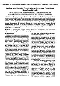
[email protected] parallelism. and encourages nearest neighbour (NN) links between adjacent PEs (NN or 4NN: links to 4 sides {east. west. north, south}, or, 8NN: NN-links to 8 sides {east, northeast, north, north-west, west, south-west, south, south-east}, like in CHESS array). Typically, longer lines are added with different lengths for connections over distances larger than 1. DP-FPGA (Datapath FPGA) [3] has been introduced to implement regularly structured datapaths. It is a FPGA-like mixed fine and coarse grained architecture with 1 and 4 bits. Its fabric includes 3 component types: control logic, the datapath, and memory. The datapath block consists of 4 bitslices: each bit-slice with a lookup table, a carry chain and a four-bit register. DP-FPGA provides separate routing resources for data (horizontal, 4 bits wide) and control signals (vertical, single bit). A third resource is the shift block to support single-bit or multi bit shifts and irregularities. The KressArray is primarily a mesh flexibility Fig. 2: Bridgof rDPUs physically connected through ing the gap. microprocessor wiring by abutment: no extra routing areas needed.. In 1995 it has been published [4] as “rDPA” (reconfigurreconfigurable able DataPath Array). “KressArray” computing has been coined later. The KressArray is a super-systolic array (generalization ASIC of the systolic array: fig. 4) which is performance achieved by DPSS (see § „DPSS“). Its interconnect fabric distinguishes 3 physical levels: multiple unidirectional and/or bidirectional NN links (fig. 3), full length or segmented column or row backbuses, a single global bus reaching all rDPUs (also for configuration). Each rDPU can serve for routing only, as an operator, or, an operator with extra routing paths. The 2nd and 3rd level is layouted over the cell: wiring by abutment capability is not affected. A first 32 bit KressArray included an additional control unit for the MoM-3 [5] Xputer [6] [7] [8] with rDPUs supporting all C language operators. With the new Xplorer environment [9] rDPUs also support any other operator repertoires including branching, while loops and do-while loops. I/O data streams from and to the array can be transferred by global bus, array edge ports, or ports of other rDPUs (addressed individually by an address generator).
Abstract. The paper gives a brief survey over a decade of R&D on coarse grain reconfigurable hardware and related compilation techniques and points out its significance to the emerging discipline of reconfigurable computing.
1.
Introduction
Rapidly increasing attendance [1] of conferences on reconfigurable computing and the adoption of this topic area by congresses like ASP-DAC, DAC, DATE, ISCAS, SPIE, and others indicate, that reconfigurable platforms are heading from niche to mainstream, bridging the gap between ASICs and microprocessors (fig. 2). It’s time to revisit R&D results: the goal of this paper. (On some projects mentioned we have only incomplete or no information on the status of implementation.)
2.
Coarse Grained Reconfigurable Architectures
Using FPGAs as accelerator platforms is not subject of this paper. In contrast to FPGA use (fine grain reconfigurable) the area of Reconfigurable Computing mostly stresses the use of coarse grain reconfigurable arrays (RAs) with pathwidths greater than 1 bit, because fine-grained architectures are much less efficient because of a huge routing area overhead and poor routability [2]. Since computational datapaths have regular structure, full custom designs of reconfigurable datapath units (rDPUs) can be drastically more area-efficient, than by assembling the FPGA way from single-bit CLBs. Coarse-grained architectures provide operator level CFBs, word level datapaths, and powerful and very area-efficient datapath routing switches. A major benefit is the massive reduction of configuration memory and configuration time, as well as drastic complexity reduction of the P&R (placement and routing) problem. Several architectures will be briefly outlined (also see figure 1). Some of them introduce multi-granular solutions, where more coarse granularity can be achieved by bundling of resources, such as e. g. 4 ALUs of 4 bits each to obtain a 16 bit ALU.
2.1 Primarily Mesh-Based Architectures Mesh-based architectures arrange their PEs in a rectangular 2-D array with horizontal and vertical connections which supports rich communication resources for efficient Project
first publ.
Source
PADDI PADDI-2 DP-FPGA KressArray Colt RaPID Matrix RAW Garp Pleiades PipeRench REMARC MorphoSys CHESS DReAM Chameleon MorphICs
1990 1993 1994 1995 1996 1996 1996 1997 1997 1997 1998 1998 1999 1999 2000 2000 2000
[24] [26] [3] [4] [9] [10] [21] [12] [14] [13] [27] [23]
[15] [16] [17] [18] [19] [20]
Architecture
Granularity
Fabrics
Mapping
intended target application
crossbar 16 bit central crossbar routing DSP crossbar 16 bit multiple crossbar routing DSP and others 2-D array 1 & 4 bit, multi-granular inhomogenous routing channels switchbox routing regular datapaths 2-D mesh family: select pathwidth multiple NN & bus segments (co-)compilation (adaptable) 2-D array 1 & 16 bit inhomogenous (sophisticated) run time reconfiguration highly dynamic reconfig. 1-D array 16 bit segmented buses channel routing pipelining 2-D mesh 8 bit, multi-granular 8NN, length 4 & global lines multi-length general purpose 2-D mesh 8 bit, multi-granular 8NN switched connections switchbox rout experimental 2-D mesh 2 bit global & semi-global lines heuristic routing loop acceleration mesh / crossbar multi-granular multiple segmented crossbar switchbox routing multimedia 1-D array 128 bit (sophisticated) scheduling pipelining 2-D mesh 16 bit NN & full length buses (information not available) multimedia 2-D mesh 16 bit NN, length 2 & 3 global lines manual P&R (not disclosed) hexagon mesh 4 bit, multi-granular 8NN and buses JHDL compilation multimedia 2-D array 8 &16 bit NN, segmented buses co-compilation next generation wireless 2-D array 32 bit (not disclosed) co-compilation tele- & datacommunication 2-D array (not disclosed) (not disclosed) (not disclosed) next generation wireless
Fig. 1: Summary of the technical details of the different coarse-grained reconfigurable architectures; Note: NN stands for “nearest neighbour”.
F:\Backups sonstige\ASP-DAC\ASP_DAC01tutorHartenstein.fm 1
Although KressArrays are dynamically partially configurable, applications tried out so far did not make use of it. The KressArray Family. Supported by an application and development tool and platform architecture space explorer (PSE) environment the basic principles of the KressArray define an entire family of KressArrays covering a wide but generic variety of interconnect resources and functional resources. A later version of this PDE environment, called (see paragraph “Xplorer,”), supports the rapid creation of RA and rPDU architectures optimized for a particular application domain (like e. g. image processing, multimedia, or others), and rapid mapping of applications onto any RA of this family. Colt [10] combines concepts from FPGAs 16 8 32 and data flow computing. It’s a 16 bit pipenet 24 [11] and relies highly on runtime rDPU reconfiguration using wormhole routing. 2 Hereby, the data stream headers hold configuration data for routing and the functionality of all PEs encountered. Colt has a Fig. 3: KressArray mesh of 16 bit IFUs (Interconnected Functional NN ports examples. Units), a crossbar switch, an integer multiplier, and six data ports. Each IFU features an ALU, a barrel shifter to support multiplication and floating point, a decision unit for flow branching, and optional delay units for pipeline synchronization. MATRIX [12] (Multiple Alu architecture with Reconfigurable Interconnect eXperiment) is a multi-granular array of 8-bit BFUs (Basic Functional Units) with procedurally programmable microprocessor core including ALU, multiplier, 256 word data and instruction memory and a controller which can generate local control signals from ALU output by a pattern matcher, a reduction network, or, half a NOR PLA. With these features, a BFU can serve as instruction memory, data memory, register-file and ALU, or independent ALU function. Instructions may be routed over the array to several ALUs. The routing fabric provides 3 levels of 8-bit buses: 8 nearest neighbour (8NN) and 4 second-nearest neighbour connections, bypass connections of length 4, and global lines. The Garp Architecture [13] resembles an FPGA and comes with a MIPS-II-like host and, for acceleration of specific loops or subroutines, a 32 by 24 RA of LUT-based 2 bit PEs. Basic unit of its primarily mesh-based architecture is a row of 32 PEs, a reconfigurable ALU. The host has instruction set extensions to configure and control the RA. Array execution is initialized by the number of clock cycles to do. Host and RA share the same memory hierarchy. Memory accesses can be initiated by the RA, but only through the central 16 columns. The blocks in the leftmost column are dedicated controllers for interfacing. For fast reconfigurations, the RA features a distributed cache with depth 4, which stores the least recently used configurations. The routing architecture includes 2 bit horizontal and vertical lines of different length, segmented in a non-uniform way: short horizontal segments spanning 11 blocks, long horizontals spanning the whole array, and different length vertical segments. RAW: Reconfigurable Architecture Workstation [14] provides a RISC multi processor architecture composed of NNconnected 32-bit modified MIPS R2000 microprocessor tiles with ALU, 6-stage pipeline, floating point unit, controller, register file of 32 general purpose and 16 floating point registers, program counter, and local cached data memory and 32 Kilobyte SRAM instruction memory. The prototype chip features 16 tiles arranged in a 4 by 4 array. Early concepts [14] having been abandoned included also configurable logic to allow customized instructions. RAW provides both a static (determined at compiletime) and a dynamic network (determined at run-time: wormhole routing for the data forwarding). Since the processors lack hardware for register renaming, dynamic instruction issuing or caching (like in superscalar processors), statically scheduled instruction streams are generated by the compiler, thus moving the responsibility for all dynamic issues to the development software. However, RAW
array applications
pipeline properties shape resources
mapping
scheduling (data stream formation)
systolic regular data linear uniform linear projection or array dependency only only algebraic synthesis supersimulated annealing, (e.g. force-directed) scheduling systolic no restrictions genetic morphing, or algorithm RA other P&R algorithm Fig. 4: Pipelined datapath arrays (pipe networks).
provides possible flow control as a backup dynamic support, if the compiler should fail to find a static schedule. REMARC (Reconfigurable Multimedia Array Coprocessor) [15], a reconfigurable accelerator tightly coupled to a MIPS-II RISC processor, consists of an 8 by 8 array of 16 bit “nanoprocessors” with memory, attached to a global control unit. The communication resources consist of nanoprocessors NN connections and additional 32 bit horizontal and vertical buses which also allow broadcast to processors in the same row or column respectively, or, to broadcast a global program counter value each cycle to all nanoprocessors, also to support SIMD operations. MorphoSys (Morphoing System [16]) has a MIPS-like “TinyRISC” processor with extended instruction set, a meshconnected 8 by 8 RA, a frame buffer for intermediate data, context memory, and DMA controller. The RA is divided into four quadrants of 4 by 4 16 bit RCs each, featuring ALU, multiplier, shifter, register file, and a 32 bit context register for storing the configuration word. The interconnect network features 3 layers: 4 NN ports, links of distance 2, and, interquadrant buses spanning the whole array. TinyRISC extra DMA instructions initiate data transfers between the main memory and the “frame buffer” internal data memory for blocks of intermediate results, 128 by 16 bytes in total.. The CHESS Array. The CHESS hexagonal array [17] features a chessboard-like floorplan with interleaved rows of alternating ALU / switchbox sequence (figure 5). Embedded RAM areas support high memory requirements. Switchboxes can be converted to 16 word by 4 bit RAMs if needed. RAMs within switchboxes can also be used as a 4-input, 4-output LUT. The interconnect fabrics of CHESS has segmented fourbit buses of different length. There are 16 buses in each row and column, 4 buses for local connections spanning one switchbox, 4 buses of length 2, and 2 buses of length 4, 8 and 16 respectively. To avoid routing congestion, the array features also embedded 256 word by 8 bit block RAMs. An ALU data output may feed the configuration input of another ALU, so that its functionality can be changed on a cycle-percycle basis at runtime without uploading. However, partial configuration by uploading is not possible. ALU
ALU
Embedded ALU
ALU
ALU
ALU
ALU
RAM
ALU
ALU
ALU
Embedded RAM
Fig. 5: CHESS array hexagon floor plan.
The DReAM Array (Dynamically Reconfigurable Architecture for Mobile Systems [18]) for next generation wireless communication, is a 0.35 µm CMOS standard cell design fabricated by Mietec/Alcatel. Each RPU consists of: 2 dynamically reconfigurable 8-bit Reconfigurable Arithmetic Processing (RAP) units, 2 barrel shifters, a controller, two 16 by
F:\Backups sonstige\ASP-DAC\ASP_DAC01tutorHartenstein.fm 2
8-bit dual port RAMs (used as LUT or FIFO), and, a Communication Protocol Controller. The RPU array fabric uses NN ports and global buses segmentable by switching boxes. Industrial RA Platforms. Chameleon Systems offers a reconfigurable platform for telecommunications and data communications [19], with a 32 bit RISC core as a host, connected to a RA fabric with 108 DPUs (84 32-bit ALUs and 24 16-bit multipliers), arranged as 4 slices by 3 tiles à 7 ALUs and 2 multipliers each, including an 8 word instruction memory for each DPU and 8 kBytes of local memory for each slice. Also MorphICs mentions its RA, but without details [20].
paths, consists of clusters of 8 arithmetic execution units (EXUs) 16 bits wide, including 8 word SRAM (which may be concatenated for 32 bits) and connected to a central crossbar switch box. Interconnect is organized in 2 levels: a 3 bit global bus to broadcast global instructions to each EXU’s controller CTL, decoded locally at second level into a 53 bit instruction word. The PADDI-2 Architecture [26] features a data-driven execution mechanism. Although the basic architectural principles of the original PADDI were kept, the PADDI-2 has several differences. It has 48 EXUs. Each PE features a 16 bit ALU also including booth multiply and select, multiplication instructions taking 8 cycles on a single processor. Alternatively, eight EXUs can be pipelined, resulting in a single cycle multiplication. PADDI-2 EXUs are packed in 12 clusters of four elements each two level interconnect: six 16 bit intracluster data buses (plus one bit control buses, and, inter-cluster 16 data buses, which can be broken up into shorter segments. The Pleiades Architecture [27] is a generalized low power “PADDI-3” with programmable microprocessor and heterogeneous RA of EXUs, which allows to integrate both fine and coarse grained EXUs, and, memories in place of EXUs. For each algorithm domain (communication, speech coding, video coding), an architecture instance can be created (with known EXU types and numbers). Communication between EXUs is dataflow driven. The control means available to the programmer are basic EXU configurations to specify its operation, and interconnect configurations to build EXU clusters. All configuration registers are part of the processor’s memory map and configuration codes are processor’s memory writes.
2.2 Architectures Based on Linear Arrays Some RAs are based on one or several linear arrays, typically also with NN connect, aiming at mapping pipelines onto it. If the pipes have forks, which otherwise would require a 2-D realization, additional routing resources are needed, like longer lines spanning the whole or a part of the array, often being segmented. Two RAs have linear array structure. RaPiD [21] provides different computing resources, like ALUs, RAMs, multipliers, and registers, but irregularly distributed. While RaPiD uses mostly static reconfiguration, PipeRench relies on dynamic reconfiguration, allowing the reconfiguration of a PE in each execution cycle. Besides the mostly unidirectional NN connects, it provides also a global bus. RaPiD: The Reconfigurable Pipelined Datapath (RaPiD) [21] aims at speed-up of highly regular, computation-intensive tasks by deep pipelines on its 1-D RA. RaPiD-1 features 15 DPUs of 8 bit with integer multiplier (32 bit output), 3 integer ALUs, 6 general-purpose datapath registers and 3 local 32 word memories, all 16 bits wide. ALUs can be chained. Each memory has a special datapath register with an incrementing feedback path. To implement I/O streams RaPiD includes a stream generator with address generators, optimized for nested loop structures, associated with FIFOs. The address sequences for the generators are determined at compile-time. RaPiD’s routing and configuration architecture consists of several parallel segmented 16 bit buses, which span the whole array. The length of the bus segments varies by tracks. In some tracks, adjacent bus segments can be merged. The sophisticated interconnect fabric cannot be detailed here. PipeRench [23], an accelerator for pipelined applications, provides several reconfigurable pipeline stages (“stripes”) and relies on fast partial dynamic pipeline reconfiguration and run time scheduling of configuration streams and data streams. It has a 256 by 1024 bit configuration memory, a state memory (used to save the current register contents of a stripe), an address translation table (ATT), four data controllers, a memory bus controller and a configuration controller. The reconfigurable fabric of the PipeRench allows the configuration of a pipeline stage in every cycle, while concurrently executing all other stages. The fabric consists of several (horizontal) stripes composed of interconnect and PEs with registers and ALUs, implemented as 3-input lookup tables. The ALU includes a barrel shifter, carry chain circuitry, etc. A stripe provides 32 ALUs with 4 bits each. The whole fabric has 28 stripes. The interconnect scheme of PipeRench features local interconnect inside a stripe as well as local and global interconnect between stripes and four global buses.
2.4 Future Reconfigurable Architectures A universal RA obviously is an illusion. The way to go is toward sufficiently flexible RAs, optimized for a particular application domain like e. g. wireless communication, image processing or multimedia etc. There is a need for tools supporting such dedicated RA architecture development. But architectures have an immense impact on implementability of good mapping tools. „Clever“ fabrics are too sophisticated to find good tools. The best solution are simple generic fabrics architecture principles, or, a mapping tool which generically creates by itself the architectures it can manage easily [9], or, a combination of both approaches like the platform space exploration (s. „The KressArray Family“ and “Xplorer,”).
3.
Programming Coarse Grain RAs
Programming frameworks for RAs (also see fig. 1) are highly dependent on structure and granularity, and differ by language level. For MorphoSys, MATRIX, PADDI-2 and REMARC it’s assembler level. Some support the designer by a graphical tool for manual P&R. Others feature automatic design flow from HDL or high-level programming language. Environments differ by the approach used for technology mapping, placement, routing. Using only a simple script for technology mapping [28] DP-FPGA [3] is not considered. Technology mapping is mostly simpler for coarse grain architectures than for FPGAs. Approaches are: direct mapping, where the operators are mapped straight forward onto PEs, with one PE for one operator, or, using an additional library of functions not directly implementable by one PE, or, more sophisticated tree matching also capable to merge several operators into one PE by a modified FPGA tool kit. An exception is the RAW compiler doing partitioning instead of technology mapping, since RAW has RISC cores as PEs accepting blocks from program input. For operator placement, the architecture has an impact. An approach often used for FPGAs synthesis is placement by simulated annealing or a genetic algorithm. Garp uses a tree matching algorithm instead, where placement is done together with technology mapping. The use of greedy algorithms is feasible only for linear arrays (PipeRench), or with a high
2.3 Crossbar-Based Architectures A full crossbar switch, a most powerful communication network is easily to rout. But the 2 RAs of this category use only reduced crossbars. PADDI for the fast prototyping of DSP datapaths features eight PEs, all connected by a multilayer crossbar. PADDI-2 has 48 PEs, but saves area by restricted crossbar with a hierarchical interconnect structure for linear arrays of PEs forming clusters. This fabrics sophistication has again an impact on routing. PADDI-1 (Programmable Arithmetic Device for DSP) [24] [25], for rapid prototyping of computation-intensive DSP data
F:\Backups sonstige\ASP-DAC\ASP_DAC01tutorHartenstein.fm 3
mapping
Kress DPSS
placement routing
simulated annealing
CHESS
RaPiD
simulated annealing Pathfinder
for the RaPiD system works similar, but relies on relatively complex algorithms. Colt tools use a structural description of the dataflow. CHESS has been programmed from a hardware description language (JHDL) source. P&R quality has a massive impact on application performance. But, due to the low number of PEs, P&R is much less complex than for FPGAs and computational requirements are drastically reduced. DPSS (DataPath Synthesis System) [4] generates configuration code for KressArrays from ALE-X high-level language sources [4] supporting datapaths with assignments, local variables and loops. After classical optimizations it generates an expression tree. Next processing steps include a front end, logic optimization, technology mapping creating a netlist, simultaneous P&R by simulated annealing, and I/O scheduling (incl. loop folding, memory cycle optimization, register file usage). The result is the application’s KressArray mapping and array I/O schedule. Finally configuration binaries are assembled. Routing is restricted to direct NN connect and rout-through of length 1. Other connect is routed to buses or segmented buses. DPSS has also been part of the MoM3 Xputer compiler accepting and partitioning a subset of C subset into sequential MoM code and structural KressArray code. The more general CoDe-X approach [31] uses this MoM compiler as part of a partitioning co-compiler accepting a C language superset and partitioning the application onto the host and one or several Xputer-based accelerators. Tools for Colt [10] accept a dataflow description (below C level) for placement by a genetic algorithm and routing by a greedy algorithm (routing congestion is cured at run-time by wormhole reconfiguration). Data stream headers hold configuration data for routing and the functionality of all PEs encountered. Programming RaPiD[21] machine Computer Xputer [9] is done in RaPiD-C, a C-like category (“v. Neumann”) (no transputer) language with extensions engine instruction data (like synchronization mechan- principles sequencing sequencing isms and conditionals to procedural sequencing identify first or last loop machine (deterministic) iteration) to explicitly speci- paradigm control-flow- data-streamdriven driven fy parallelism, data movement and partitioning, RaPiD-C RA no yes programs may consist of supported Fig. 7: Machine Paradigms. several nested loops describing pipelines. Outer loops are transformed into sequential code for address generators, inner loops into structural code for the RA. The compilation steps are: netlist generation from structural code, extraction of dynamic control, generation of controller code instruction streams for dynamic control and generation of I/O configuration data for the stream units. The netlist is mapped onto RaPiD by pipelining, retiming, and P&R. Placement is done by simulated annealing, with routing (by pathfinder [29]) done on the fly to measure placement quality [32]. For Programming the CHESS array [17] a compiler [33] has been implemented accepting JHDL [34] sources and generating CHESS netlists. Placement is done by simulated annealing and routing by Pathfinder’s negotiated congestion algorithm [29]. Part of the work is not disclosed.
Colt genetic algorithm greedy algorithm
Fig. 6: FPGA-Style Mapping for coarse grain reconfigurable arrays.
level communication network (RAW). PADDI is an exception by using a scheduling algorithm for resource allocation. Routing also features quite different approaches. In two cases, the routing is not done in an extra phase but integrated into the placement and done on the fly. One approach (KressArray) uses a simple algorithm restricted to connects with neighbours and targets with at most the distance of one. The other (RaPiD) employs the pathfinder algorithm [29], which has been developed for FPGA routing. Greedy routing would be not satisfying. General exceptions to the routing approaches is the RAW architecture, which features only one high-level communication resource, so no selection of routing resources is needed, and the PADDI architecture, which features a crossbar switch having the same effect. Greedy routing algorithms are only used for 1-D RAs, or architectures capable to cure routing congestion by other mechanisms, like Colt with wormhole run-time reconfiguration.
3.1 Assembler Programming Assembler level code for coarse grain architectures can be compared to configuration code for FPGAs. In the case of systems comprising a microprocessor / RA symbiosis, only the reconfigurable part is considered for the classification. Programming is done mainly at a kind of assembler level for PADDI-2, MATRIX, and, RAs of REMARC and MorphoSys. PADDI-2 is crossbar-based whereas the rest is mesh-based. Programming PADDI-2. For programming PADDI-2 [26], a tool box has been developed which includes software libraries, a graphical interface for signal flow graphs, routing tools, simulation tools, compilation tools and tools for board access and board debugging. Major parts of this process are done manually. The input specifies assembly code for each function in the signal flow graph. The programmer manually partitions the signal flow graph with a graphical tool, which also aids in manual placement and routing. As an alternative to manual placement and routing, an automated tool is provided, which guarantees to find a mapping, if one exists, by exhaustive methods which need much computation time. For Programming MATRIX [12] an assembly level macro language has been developed. Some work on P&R pointed out the original MATRIX’s weak points [30]. REMARC tools [15] allow concurrent programming of the RISC processor (by C using the GCC compiler) and the RA by adding REMARC assembler instructions. The compiler then generates assembly code for the RISC processor with the REMARC assembler instructions embedded which are further processed by a special REMARC assembler generating binary code for the REMARC instructions. Finally, the GCC compiler is used again to generate RISC instruction code to invoke REMARC and its instructions embedded as binary data. Programming MorphoSys is supported by a SUIF-based compiler [16] for host, and development tools for RA. Host / RA partitioning is done manually by adding a prefix to functions to be mapped onto RA. The compiler generates TinyRISC code for RA activation. Configuration code is generated via a graphical user interface or manually from an assembler level source also usable to simulate the architecture from VHDL.
3.3 Other mapping approaches Greedy algorithms are poor in mapping to FPGAs. But, although Garp is mesh-based, mapping treats it like a linear array which allows mapping in one step by a simple greedy routing algorithm. RAW features only one communication resource, removing the wire selection problem from routing. Instead, the compiler schedules time multiplexed NN connections. CPU cores inside RAW PEs simplify mapping by loading entire source code blocks. PipeRench resembling a linear array and interconnect fabrics restrictions keep placement simple for a greedy algorithm. PADDI uses a standard P&R approach. Garp tools [13] use a SUIF-based C compiler [35] to generate code for the MIPS host with embedded RA configuration code to accelerate (only non-nested) loops. At next basic blocks are
3.2 Frameworks with FPGA-Style Mapping Computation-intensive algorithms for mapping onto FPGAs are well-known and can often be used directly for coarse grain architectures like for CHESS, Colt, KressArray, RaPiD (see fig. 6). All four use simulated annealing or other genetics for placement, and two use pathfinder for routing [29]. The KressArray DPSS (Datapath Synthesis System) accepts a C-like language source. The compilation framework
F:\Backups sonstige\ASP-DAC\ASP_DAC01tutorHartenstein.fm 4
inter- status evaluation status generation Explorer System year source active 1991 [49] no abstract models rule-based DPE Clio 1992 [50] yes prediction models advice generator DIA 1998 [51] yes prediction fr. library rule-based DSE for RAW 1998 [41] no analytical models analytical ICOS 1998 [52] no fuzzy logic greedy search DSE f. Multimedia 1999 [53] no simulation branch and bound Xplorer 1999 [9][42] yes fuzzy rule-based simulated annealing Fig. 8: Design Space Exploration Systems.
generated and converted into hyperblocks containing a contiguous group of basic blocks, also from alternative control paths. Control flow inside a hyperblock is converted for predicated execution. Blocks, which cannot be mapped, are removed from hyperblocks. The resulting reduced hyperblock is then the basis for mapping. The next step generates interfacing instructions for the host, and transforms the hyperblock into a DFG (data flow graph). The proprietary Gamma tool [36] maps the DFG onto Garp using a tree covering algorithm which preserves the datapath structure, supports features like the carry chains. Gamma first splits the DFG into subtrees and then matches subtrees a with module patterns which fit in one Garp row. During tree covering, the modules are also placed in the array. After some optimizations the configuration code is generated (incl. outing [38]), assembled into binary form, and, linked with the hosts C object code. RAW tools [39] [40] include a SUIF-based C compiler and a run-time system managing dynamic mechanisms like branch prediction, data caching [41], speculative execution, dynamic code scheduling. The compiler handles resource allocation, parallelism exploitation, communication scheduling, code generation (for host and switch processors in each tile), and, divides execution into coarse-grain parallel regions internally communicating by static network, whereas intra-region communication uses messages. The phases are: pointer analysis [39] with data dependency analysis and memory access generation (if known at compile-time), partitioning application data for distributed memory; space-time scheduling [40] for parallelization; address translation for caching by software. RAW binary is generated by the MIPS compiler back end. The RAW project aims more at parallel processing rather than reconfigurable computing and failed in finding a good automatic mapping algorithm [42]. PipeRench tools [23] [43] use the DIL single-assignment (SA) language for design entry and as an intermediate form. First, the compiler inlines all modules, unrolls loops and generates a straightline SA program (SAP). After optimizations and breaking the SAP into pieces fitting on one stripe, a greedy P&R algorithm is run which tries to add nodes to stripes. Once placed, a node is routed and never moved again. P&R is fast by crossbar switch usage, coarse granularity, and, restriction to unidirectional pipelines. CADDI [44], assembler and simulator, has been implemented for PADDI. First a silage [45] specification is compiled into a CDFG (control /data flow graph), used for estimations of critical path, minimum and maximum bounds for hardware for a given time allocation, minimum bounds of execution time, and for transformations like pipelining, retiming, algebraic transformations, loop unrolling and operation chaining. CDFG to architecture technology mapping is straight-forward since all components are fixed and routing through crossbars is efficient. If several PADDI clusters are involved, a partitioning step comes before resource allocation, assignment, and scheduling. The assignment phase maps operations to EXUs by a rejectionless antivoter algorithm [46]. Compilation for Pleiades. Because of the complex design space created by the heterogeneous architecture, the application mapping problem is not yet solved completely. Commercially available platforms. Chameleon Systems uses co-compilation [19] (like known from earlier work [36] [43] [31] [47] [48]), combining compiler optimization and multithreading techniques, to hide configuration loading latency and list scheduling to find ’best’ schedule for a series of eBIOS calls. About mapping or compilation techniques for the MorphICs RA no information has been disclosed.
4.
provide only predictions etc. from a knowledge data base. Advanced DSEs provide status generation, e g. by expert system, and present advice like a choice of proposals. Noninteractive DSEs automatically generate a solution status from rule-based knowledge or fuzzy learning.
4.1 Design Space Exploration Interactive design assistants are DPE and Clio (both for VLSI) and DIA. Including effect predictors and proposal generators DPE (Design Planning System) [49] (using an expert system), Clio [50] (using a hierarchy of templates) and DIA (DatapathIntensive ASICs) [51] (targeting semi-custom ASIC behavioural level and based on encapsulated expert knowledge), generate a design flow by creating a schematic, a data flow graph, or a layout from a specification and area, cycle time, power, e.a. constraints and to improve area, power, throughput etc.
4.2 Platform Space Explorers (PSEs) A PSE serves to find an optimum RA or processor array (PA) platform for an application domain by optimizing array size, path width, processor’s MIPS, number of ALUs and branch units, local SRAM size, data and instruction cache sizes, local bandwidth, interconnect latency etc. from requirements like chip area, total computation, memory size, buffer size, communication etc. Software or configware application programming is finally not part of exploration, but may serve platform evaluation. All three being non-interactive, the DSE [41] for RAW [14] featuring an analytical model, ICOS (Intelligent Concurrent Object-oriented Synthesis) [52] featuring object-oriented fuzzy techniques, and “DSE for Multimedia Processors” [53] (DSEMMP) aim at automatic synthesis of a multiprocessor platform from system descriptions, performance constraints, and a cost bound and generate an architecture. . DSEMMP aims at shared memory with intel Strong-ARM SA-110 as a starting point. Xplorer, an interactive PSE framework [9] [42] has been implemented around the DPSS mapper [4]. This universal design space exploration environment supports both, optimum architecture selection (e. g. domain-specific) and application development onto it and includes several tools: architecture editor (to edit communication resources and annealing parameters), mapping editor (to change I/O port type, freeze locations of edge port, cell or cell group etc.), instruction mapper to change the operator repertoire, architecture suggestion generator [54], HDL generator for cell simulation, retargettable cell layout generator (planned, similar to [55]), power estimator (planned [56], similar to [58]). A cycle through an exploration loop usually takes only minutes, so that a number of alternative architectures may be checked in a reasonable time. By mapping the application onto it verification is provided directly.
5.
Conclusions
Exploding ASIC design cost and shrinking ASIC product life cycles are a motivation to replace at least some of the ASICs by RAs for product longevity by upgrading [59] [60] [61]. Performance is only one part of the story. The design community is far away from fully exploiting the flexibility of RAs [34], supporting novel powerful techniques -directly in system jointly with all other components in real time, dramatically faster than simulation- for debugging, run-time profiling, verification, system-wide tuning, run-time API, field-
Design Space Explorers (DSEs)
Some development environments aim beyond compiling. DSEs (fig. 8 [42]) select one of many alternative solutions to meet a design goal meeting constraints or desired properties to optimize a design or a (by PSE) programmable platform. Guidance systems or design assistants are interactive DSEs giving advice during the design flow. Some DSEs avoid the status generation and
F:\Backups sonstige\ASP-DAC\ASP_DAC01tutorHartenstein.fm 5
maintenance, field-upgrades (also via internet) flexible selfmonitoring functions by configuring unused parts of the RA. time of “Instruction Fetch” fetch“ time of „instruction This potential is largely unrealized although having been technically possible run microprocessor and demonstrated already for about arun time time parallel computer decade [34]. Using RAs for ASICs loading creates new markets transferring loading time time synthesis from vendor to customer, compile Reconfigurable Computing who needs hardware experts compile or time time compilers to replace CAD. A machine fabrication fabrication time time ASIC paradigm makes compilers much easier to develop and machines easier to Fig. 9: “Instruction Fetch”. program - the success story of software industry. But “v. Neumann” does not support soft datapaths because “instruction fetch” is not done at run time (fig. 9). Instead of a program counter we need a data counter [63] (data sequencer [64]): the new “Xputer” machine paradigm for soft hardware (fig. 7) [7]. Instead of a “control flow” sublanguage a “data stream” sublanguage defines data goto, data jumps, data loops (also nested), parallel data loops (using multiple data counters) like by the MoPL language [65] - easy to learn by its similarity to control flow. Reconfigurable platforms and their applications are heading from niche to mainstream, bridging the gap between ASICs and microprocessors. It’s time to revisit R&D results and to derive commercial solutions: at least one promising approach is available. It is time for you to get involved.
6.
25. D. C. Chen, J. M. Rabaey: A Reconfigurable Multiprocessor IC for Rapid Prototyping of Algorithmic-Specific High-Speed DSP Data Paths; IEEE J. Solid-State Circuits, Vol. 27, No. 12, Dec. 1992. 26. A. K. W. Yeung, J.M. Rabaey: A Reconfigurable Data-driven Multiprocessor Architecture for Rapid Prototyping of High Throughput DSP Algorithms; Proc. HICSS-26, Kauai, Hawaii, Jan. 1993. 27. J. Rabaey: Reconfigurable Computing: The Solution to Low Power Programmable DSP; Proc. ICASSP’97 Munich, Germany, April 1997. 28. D. Lewis: Personal Communication, April 2000. 29. C. Ebeling et al.: Placement and Routing Tools for the Tryptich FPGA; IEEE Trans VLSI Systems 3, No. 4, December 1995. 30. A. DeHon: Personal Communication, February 2000. 31. J. Becker: A Partitioning Compiler for Computers with Xputer-based Accelerators; Ph. D. dissertation, Kaiserslautern University, 1997. 32. C. Ebeling: Personal Communication, March 2000. 33. A. Marshall: Personal Communication; February 2000. 34. B. Hutchings, B. Nelson: Using General-Purpose Programming Languages for FPGA Design; Proc. DAC 2000, Los Angeles, June 2000 35. M. W. Hall et al.: Maximizing Multiprocessor Performance with the SUIF Compiler; IEEE Computer, Dec. 1996 36. T. J. Callahan and J. Wawrzynek: Instruction-Level Parallelism for Reconfigurable Computing; in [37] pp. 248-257. 37. R. Hartenstein, A. Keevallik (Editors): Proc. FPL’98, Tallinn, Estonia, Aug. 31- Sept. 3, 1998, LNCS, Springer Verlag, 1998 38. J. Hauser: Personal Communication, March 2000. 39. R. Barua et al.: Maps: A Compiler-Managed Memory System for RAW Machines; Proc. ISCA‘99, Atlanta, USA, June, 1999. 40. W. Lee et al.: Space-Time Scheduling of Instruction-Level Parallelism on a RAW Machine; Proc. ASPLOS‘98, San Jose, Oct. 4-7, 1998. 41. C. A. Moritz et al.: Hot Pages: Software Caching for RAW Microprocessors; MIT, LCS-TM-599, Cambridge, MA, Aug. 1999. 42. U. Nageldinger: Design-Space Exploration for Coarse Grained Reconfigurable Architectures; dissertation, Kaiserslautern University, 2000 43. M. Budiu and S. C. Goldstein: Fast Compilation for Pipelined Reconfigurable Fabrics; Proc. FPGA‘99, Monterey, Feb. 1999, pp. 135-143. 44. D. Chen at al.: An Integrated System for Rapid Prototyping of High Performance Data Paths; Proc. ASAP‘92, Los Alamitos, Aug. 4-7, 1992 45. P. H. Hilfinger: A High-Level Language and Silicon Compiler for Digital Signal Processing; Proc. 1985 IEEE CICC., Portland, May 20-23, 1985. 46. M. Potkonjak, J. Rabaey: A Scheduling and Resource Allocation Algorithm for Hierarchical Signal Flow Graphs; Proc. DAC‘89, Las Vegas, June 25-29, 1989 47. M. Weinhardt, W. Luk: Pipeline Vectorization for Reconfigurable Systems; Proc. IEEE FCCM, April 1999 48. M. Gokhale, J. Stone: NAPA C: Compiling for a hybrid RISC / FPGA architecture; Proc. IEEE FCCM April 1998 49. D Knapp, A. Parker: The ADAM Design Planning Engine, IEEE Trans CAD 10/7, July 1991 50. J. Lopez et al.: Design Assistance for CAD Frameworks; Proc. EURODAC’62, Hamburg, Germany, Sept. 7-10, 1992 51. L. Guerra et al.: A Methodology for Guided Behavioural Level Optimization; Proc. DAC’98, San Francisco, June 15-19, 1998 52. P.-A. Hsiung et al.: PSM: An Object-oriented Synthesis Approach to Multiprocessor Design; IEEE Trans VLSI Systems 4/1, March 1999 53. J. Kin et al.: Power Efficient Media Processor Design Space Exploration; Proc. DAC’99, New Orleans, June 21-25, 1999 54. R. Hartenstein, M. Herz, T. Hoffmann, U. Nageldinger: Generation of Design Suggestions for Coarse-Grain Reconfigurable Architectures; in [1] 55. V. Moshnyaga, H. Yasuura: A Data-Path Modules Design from Algorithmic Representations; IFIP WG 10.5 Worksh. on Synthesis, Generation and Portability of Library Blocks for ASIC Design, Grenoble, France, Mar 1992 56. U. Nageldinger et al.: Design-Space Exploration of Low Power Coarse Grained Reconfigurable Datapath Array Architectures; in [57] 57. D. Soudris, P. Pirsch, E. Barke (Editors): Proc. PATMOS 2000; Göttingen, Germany Sept. 13 - 15, 2000; LNCS, Springer Verlag, 2000 58. L. Kruse et al.: Lower Bounds on the Power Consumption in Scheduled Data Flow Graphs with Resource Constraints; Proc. DATE, Mrch 2000. 59. T. Kean: It‘s FPL, Jim - but not as we know it! - Market Opportunities fro the new Commercial Architectures; in [1] 60. H.Fallside, M.Smith: Internet Connected FPL; in [1] 61. R. Hartenstein, M. Herz, T. Hoffmann, U. Nageldinger: An Internet Based Development Framework for Reconfigurable Computing; in [62] 62. P. Lysaght, J. Irvine, R. Hartenstein (Eds.): Proc. FPL'99, Glasgow, UK, Aug./Sept. 1999, LNCS Vol. 1673, Springer-Verlag, 1999 63. J. Becker et al.: A General Approach in System Design Integrating Reconfigurable Accelerators; Proc. IEEE ISIS’96; Austin, TX, Oct. 9-11, 1996 64. M. Herz, et al.: A Novel Sequencer Hardware for Application Specific Computing; Proc. ASAP‘97, Zurich, Switzerland, July 14-16, 1997 65. A. Ast, J. Becker, R. Hartenstein, R. Kress, H. Reinig, K. Schmidt: Data-procedural Languages for FPL-based Machines; in [66] 66. R. Hartenstein, M. Servit (Editors): Proc. FPL’94, Prague, Czech Republic, Sept. 7-10, 1994, LNCS, Springer Verlag, 1994
Literature
1. R. Hartenstein, H. Grünbacher (Editors): The Roadmap to Reconfigurable computing - Proc. FPL2000, Aug. 27-30, 2000; LNCS, Springer-Verlag 2000 2. R. Hartenstein: The Microprocessor is no more General Purpose (invited paper), Proc. ISIS'97, Austin, Texas, USA, Oct. 8-10, 1997. 3. D. Cherepacha and D. Lewis: A Datapath Oriented Architecture for FPGAs; Proc. FPGA‘94, Monterey, CA, USA, February 1994. 4. R. Kress et al.: A Datapath Synthesis System for the Reconfigurable Datapath Architecture; ASP-DAC'95, Chiba, Japan, Aug. 29 - Sept. 1, 1995 5. H. Reinig: A Scalable Architecture for Custom Computing; Ph.D. Thesis, Univ. of Kaiserslautern, Germany, July 1999. 6. R. Hartenstein, A. Hirschbiel, M. Weber: MoM - a partly custom-design architecture compared to standard hardware; IEEE CompEuro 1989 7. R. Hartenstein et al.: A Novel Paradigm of Parallel Computation and its Use to Implement Simple High Performance Hardware; InfoJapan’90, 30th Anniversary o’Computer Society of Japan, Tokyo, Japan, 1990. 8. R. Hartenstein et. al.: A Novel ASIC Design Approach Based on a New Machine Paradigm; IEEE J.SSC, Volume 26, No. 7, July 1991. 9. U. Nageldinger et al.: KressArray Xplorer: A New CAD Environment to Optimize Reconfigurable Datapath Array Architectures; ASPDAC, Yokohama, Japan, Jan. 25-28, 2000. 10. R. A. Bittner et al.: Colt: An Experiment in Wormhole Run-time Reconfiguration; SPIE Photonics East `96, Boston, MA, USA, Nov. 1996. 11. K. Hwang: Advanced Computer Architecture; McGraw-Hill, 1993. 12. E. Mirsky, A. DeHon: MATRIX: A Reconfigurable Computing Architecture with Configurable Instruction Distribution and Deployable Resources; Proc. IEEE FCCM‘96, Napa, CA, USA, April 17-19, 1996. 13. J. Hauser and J. Wawrzynek: Garp: A MIPS Processor with a Reconfigurable Coprocessor; Proc. IEEE FCCM‘97, Napa, April 16-18, 1997. 14. E. Waingold et al.: Baring it all to Software: RAW Machines; IEEE Computer, September 1997, pp. 86-93. 15. T. Miyamori and K. Olukotun: REMARC: Reconfigurable Multimedia Array Coprocessor; Proc. ACM/SIGDA FPGA‘98, Monterey, Feb. 1998. 16. H. Singh, et al.: MorphoSys: An Integrated Re-configurable Architecture; Proceedings of the NATO RTO Symp. on System Concepts and Integration, Monterey, CA, USA, April 20-22, 1998. 17. A. Marshall et al.: A Reconfigurable Arithmetic Array for Multimedia Applications; Proc. ACM/SIGDA FPGA‘99, Monterey, Feb. 21-23, 1999 18. J. Becker et al.: Architecture and Application of a Dynamically Reconfigurable Hardware Array for Future Mobile Communication Systems; Proc. FCCM’00, Napa, CA, USA, April 17-19, 2000. 19. X.Tang, et al.: A Compiler Directed Approach to Hiding Configuration Loading Latency in Chameleon Reconfigurable Chips; in [1] 20. http://www.MorphICs.com 21. C. Ebeling et al.: „RaPiD: Reconfigurable Pipelined Datapath“, in [22] 22. M. Glesner, R. Hartenstein (Editors): Proc. FPL’96, Darmstadt, Germany, Sept. 23-25, 1996, LNCS 1142, Springer Verlag 1996 23. S. C. Goldstein et al.: PipeRench: A Coprocessor for Streaming Multimedia Acceleration; Proc. ISCA‘99, Atlanta, May 2-4, 1999 24. D. Chen and J. Rabaey: PADDI: Programmable arithmetic devices for digital signal processing; VLSI Signal Processing IV, IEEE Press 1990.
F:\Backups sonstige\ASP-DAC\ASP_DAC01tutorHartenstein.fm 6