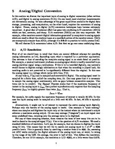
Analogue to Digital Conversion A2D maps a continuous signal to a discreet signal (set of real numbers). Practically, A2D maps an electrical input (voltage/current) to a numeric value within a given interval.
5 ds
0 continuous signal
time
dt
quantization
Parameters and requirements for A2D Sampling Rate Sampling rate is the temporal rate at which data is sampled. Sampling rate is the speed at which the digitizer’s ADC converts the input signal, after the signal has passed through the analog input path, to digital values. Hence, the digitizer samples the signal after any attenuation, gain, and/or filtering has been applied by the analog input path, and converts the resulting waveform to digital representation. The sampling rate of a high-speed digitizer is based on the sample clock that controls when the ADC converts the instantaneous analog voltage to digital values.
Sampling of a sine wave using a 3 bit digitizer
National Instruments, analog sampling basics
http://zone.ni.com/devzone/cda/tut/p/id/3016#toc1
Parameters and requirements for A2D Quantization Quantization is defined as the process of converting an analog signal to a digital representation. The inherent uncertainty in digitizing an analog value is referred to as the Quantization error. The quantization error depends on the number of bits in the converter, along with its errors, noise, and non-linearities.
a 3-bit ADC divides the range into eight divisions.The ADC translates each measurement of the analog signal to one of the digital divisions. Figure 10 shows a 5 kHz sine wave digital image obtained by a 3-bit ADC. However, increasing the resolution to 16 bits to increase the ADC number of divisions from eight to 65,536 allows the 16-bit ADC to obtain an extremely accurate representation of the analog signal.
Parameters and requirements for A2D Aliasing If a signal is sampled at a sampling rate smaller than twice the Nyquist frequency, false lower frequency component(s) appears in the sampled data. This phenomenon is called Aliasing.
A 5 MHz sine wave digitized by a 6 MS/s ADC. The dotted line indicates the aliased signal recorded by the ADC. The 5 MHz frequency aliases back in the pass-band, falsely appearing as a 1 MHz sine wave.
Parameters and requirements for A2D Nyquist Theorem Sampling rate (f s) > 2 * highest frequency component (of interest) in the measured signal The Nyquist theorem states that a signal must be sampled at a rate greater than twice the highest frequency component of interest in the signal to capture the highest frequency component of interest; otherwise, the high-frequency content will alias at a frequency inside the spectrum of interest (pass-band).
..only B correctly captures the form of the input signal
Parameters and requirements for A2D Resolution granularity of the digital values Integral Non-Linearity proportionality of output to input 1:1ideal Differential Non-Linearity uniformity of digitization increments
ds
Conversion time/Integration time how much time to convert signal to digital value dt Count-rate performance and throughput how quickly a new conversion can begin after a previous event dc Stability how much values change with time dT
Parameters and requirements for A2D Resolution Input range and number of bits quantum = DV = (Vmax-Vmin)*2-N referred to as “1LSB” (least significant bit) eg 10 bits = 210 = 1024, Vmax-Vmin = 1V => DV = 1V/1024 » 1mV The resolution is usually expressed as bits (n) and the number of steps is 2 to the power n. A converter with 12bit resolution, for instance, divides the range into 2 12, or 4096, steps. In this case a 0-10 V range will be resolved to 0.25 mV, and a 0-100 mV range will be resolved to 0.0025 mV
ideal
real: noise
Vin R1 Vout = Vin * R2/(R1+R2) R2
Parallel A2D
Input is compared simultaneously against a set of comparators -2n comparators required for n bits -threshold value defined by resistor chain
-> short conversion time -> limited resolution
Successive approximation A2D A successive approximation converter works by first comparing the input with a voltage which is half the input range. If the input is over this level it compares it with three-quarters of the range, and so on. Twelve such steps gives 12-bit resolution. While these comparisons are taking place the signal is frozen in a sample and hold circuit. After A-D conversion the resulting bytes are placed into either a pipeline or buffer store. A pipeline store enables the A-D converter to do another conversion while the previous data is transferred to the computer.
Algorithm: Generate a V ref = dV x (2n-1, 2n-2, .. , 20) in n steps Set bit = 1 If Vin > Vref bit =1 else bit = 0
--> high resolution and fast
Sigma-delta A2D Process: At t = 0 assume Vref = 0 Vout high Integrator charges at rate ~ Vin Comparator flips Counter goes low Clock increments (repeat) Vin = 0 -> output = 00000… Vin = 0.5Vin(max) -> output = 10101010…. Vin = Vin(max) -> output = 111111… The higher the input voltage, the more 1s at the serial digital output… ->high accuracy ->good linearity
Digital 2 Analogue Conversion
Example: summing amplifier R0 = 2*R1 = 4*R2 = 8*R3
->OK for a few bits ->difficult for large N
…. use of a cathode-ray tube to perform 7-bit analogue to digital conversion, outputting a serial binary data stream from an analogue input…The signal of each channel is sampled every 125 microseconds and the outputs from 12 channel modulators form a pulse-amplitude modulated T.D.M. system. Because the operation of the coder takes longer than 10.4 microseconds two coders are provided, each dealing with alternate channels…
When-the electron beam is switched on it is deflected by the stored sample voltage to the corresponding vertical height and is moved across the aperture plate by a linear sweep. As the beam passes the holes in the aperture plate current flows to the collector plate producing the coded group of output pulses; the beam is switched off and retraced in readiness for coding the next sample. In front of the aperture plate is the quantizing grid of 129 wires between which are spaces in line with the row of holes in the aperture plate. The wires are used to centre the beam accurately on a row of holes in the aperture plate: without it the beam might wander between two rows during the scan and false coding would result. During the scan a bias voltage is applied which tends to move the beam upward, but when it strikes one of the wires of the quantizing grid secondary electrons are emitted which are attracted to the collector. The signal from the collector is fed back to the vertical amplifier and deflects the beam downwards so that it is kept in a stable position just beneath the quantizing wire…
Practical: interfacing to an analogue sensor
5V
5V
Micro Vout
Processor AD input pin
Vout
Sensor output
0V
0V