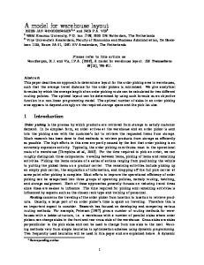
A Twisted-Bundle Layout Structure for Minimizing Inductive Coupling Noise* Guoan Zhong, Cheng-Kok Koh, and Kaushik Roy School of Electrical and Computer Engineering Purdue University, West Lafayette, IN 47907-1285 { zhongg,chengkoh,kaushik}@ecn.purdue.edu
ABSTRACT In this paper, we propose a novel misted-bundle layout structure for minimizing inductive coupling noise. In this structure, we create several routing regions and re-order the routing of nets in each of these routing regions. The purpose is to create complementary and opposite current loops in the twisted-bundle layout structure, such that the magnetic fluxes arising from any signal net within a misted group cancel each other in the current loop of a net of interest. The effectiveness of the twisted-bundle structure in minimizing coupling inductance has been verified by the application of FastHenry extraction on a 16-bit bus structure. We achieve about two orders of magnitude reduction in inductive coupling. SPICE simulations also show that the 16-bit twisted-bundle bus structure is able to maintain high signal integrity at high frequency of operation.
1. INTRODUCTION Continued scaling of semiconductor technology has brought the issues of interconnect-limited designs to the forefront. The International Technology Roadmap for Semiconductor (ITRS)[l] forecasts that as the VLSI technology advances towards giga-Hertz onchip frequency and system-level integration on larger die size, selfand coupling-inductances are becoming dominant factors in determining signal delay and signal integrity. Ref. [16] gave an extensive survey of various noise sources in circuit design. Predominantly, existing studies focused on crosstalk noise due to capacitive coupling. Due to the short range effect of capacitive coupling, techniques such as shielding, net ordering or track permutation have proved to be effective in minimizing capacitive cross-talk noise [6; 171. On the other hand, inductive effects have a long range effect because they arise from the electromagnetic phenomenon of magnetic flux linking current loops. As a result, inductive noise has a much wider spatial effect than that of a capacitive noise. For this reason, it makes the worst case situation in a circuit much harder to predict. Many of the existing studies that dealt with on-chip inductive effects focused primarily on the modeling and extraction of on-chip interconnect inductance. In [15], loop inductance was calculated in terms of partial inductances defined for wire segments. The Partial Element Equivalent Circuit (PEEC) model was widely used to analyze on-chip inductance [7; 14; 41. In [9], frequency dependent inductance and resistance were computed based on the magnetquasistatic assumption, and in [lo], a simple layout rulebased method was used to speed up the computation. *This research is supported in part by SRC (99-TJ-689), NSF (CAREER Award CCR-9984553), and a grant from Intel Corporation.
0-7803-6445-7/00/$10.00 0 2000 IEEE
A few recent studies have reported success in minimizing the undesirable inductive effects. In recent Alpha chip designs [2], onchip inductance was limited by sandwiching lines with high current density between isolating metal planes. In [l l], the wiring overhead was reduced by using a interdigitated layout structure, in which a wide wire was split into many lines, interspersed with ground lines. These techniques, however, considered only selfinductance. In [8],inductive coupling noise was reduced by shield insertion and net ordering. In this paper, we propose a novel twisted-bundle layout structure for minimizing inductive coupling noise. By creating complementary and opposite current loops in the layout structure, we achieve two orders of magnitude reduction in inductive coupling. The abilities of the twisted-bundle structure in minimizing coupling inductance and maintaining high signal integrity have been verified by the applications of FastHenry extraction and SPICE simulations on a 16-bit bus structure. The rest of the paper is organized as follows. In Section 2, preliminaries regarding inductive coupling are explained. In Section 3, we introduce a twisted-pair layout structure, upon which the twisted-bundle structure is based. In Section 4, we present the novel twisted-bundle structure and a systematic approach for synthesizing such a structure. In Section 5, we apply this structure to a 16-bit bus design and compare it with the “traditional” design based on the parasitic parameters extracted by FastHenry and the simulation results by SPICE. Finally, we conclude in Section 6.
2. PRELIMINARIES Mutual inductances, as well as self inductance, are electromagnetic phenomena that arises from current loops [12; 131. The inductances for a system of N loops are defined as:
where vi, is the magnetic flux in loop i due to a current I j in loop j . Lii represents the self inductance of loop i, whereas Li,(i # j ) represents the mutual inductance between loops i and j . According to the Faraday’s law, the mutual inductance can be calculated by finding the magnetic flux linking one loop related to per unit of current in the other loop:
where B is the density of the magnetic flux arising from current I, in loop i and the integration is over the surface of loop i. On-chip signal nets form loops with their current return paths; these loops determine the inductances as shown in Eqns. (1) and (2). Therefore, in order to accurately calculate the inductances of
406
Authorized licensed use limited to: Purdue University. Downloaded on July 9, 2009 at 14:59 from IEEE Xplore. Restrictions apply.
Mdgnetic bield
I I
signal 2
I
Mdgnetic [ield
\ \
_ _ _ _ - - - -I- - - - - - - _ _ -----___ _ _ _ _ -.
.-?- _ _ _‘_._________ _ __________>-2??-b--*
e--
around
______
from loop1 1, and the magnetic flux linkage in S22 is primarily due to loop12. As the current directions in loop11 and loop12 are opposite, the directions of the magnetic fluxes in S2l and S22 are opposite. Therefore, the two integrations over S21 and S22 cancel each other:
-_
2321
loop2
Hence, the mutual inductance between signals 1 and 2 is zero:
I
Figure 1: Twisted-pair structure. on-chip interconnections, it is of critical importance to determine the current return paths of on-chip signal nets. However, it is extremely difficult to find accurate return paths for signal nets, because in the complex interconnection structures that we deal with today, there are several paths through which a current returns [3]. In this work, we assume that all signals use the nearest power/grou nd line as their return paths [ 5 ] . Although quiet or opposite-switching neighboring nets may also serve as return paths, they are not ideal because currents returning from signal wires have to go through devices, which typically have a resistance of several hundred Ohms.
3. TWISTED-PAIRLAYOUT STRUCTURE From the Faraday’s law, there are two possible ways of eliminating the coupling inductance: (i) by creating a magnetic flux that is of an opposite direction; (ii) by eliminating or minimizing the surface area of the second loop. To achieve that, we propose a simple twisted-pair layout structure (Figure 1) that is inspired by the twisted-pair wire structure. As shown in Figure 1, we consider two signal lines in this structure. For each signal line, we assume that there exists a ground line nearby, serving as the signal’s dedicated return path. The signal and ground lines are drawn with different shades of gray. Like the twisted-pair wire structure,we intertwine one signal line and its return path at their mid-points such that they are “symmetric” about the mid-points. As the signal and ground lines co-exist on the same metal layer, the physical layout of such a twisted-pair structure involves vias and doglegs. As indicated in Figure 1, signal lines 1 and 2 form respectively loops loop1 and loop2 with their dedicated return paths. As signal 1 and its return path are twisted, loop1 is divided into two smaller loops: loop11 and Ioop12. In quasi-static condition, the current is continuous everywhere along a signal line. Therefore, the two current loops flow in opposite directions, and the magnetic fields caused by loop11 and loop12 are equal in magnitude, but in opposite directions. According to the Faraday’s law in Eqn. (2), the mutual inductance M = L21 can be calculated by finding the magnetic flux linking loop1 to loop2:
In fact, loop12 also contributes to the magnetic flux linkage in S2l. So does loop11 to S22. However, their contributions are quite insignificant, as these two components of magnetic flux also cancel each other in the integration. We can similarly argue that L12 is zero because the surfaces of the two loops loop11 and loopl2 actually “sum” to zero. All the preceding discussions are based on the assumption that the current in a signal line is continuous everywhere. However, this assumption is not valid when the wire length is sufficiently long for the transmission line effect to kick in. If parallel termination is adopted at the receiving ends of signal lines, there are no or minimal reflections at the receiving ends. Consequently, noises gathered at the victim nets cancel each other when they reach the receiving ends. Hence, the mutual inductance is still zero. We use FastHenry [9] to verify the effectiveness of the proposed twisted-pair layout structure in minimizing coupling inductance. The wire width, height, length, and spacing are l p , 2 p , 2 0 0 p . and l p , respectively. We extract the inductance matrix under two frequencies: a high frequency of fH = 1OI6Hzand a low frequency of fL = 106Hz.The inductance matrices for a normal or un-twisted structure are given below:
(
fH = 10’6HZ 7.4e - 11 6.2e - 12 6.2e - 12 7.4e - 11
fL = 106Hz 9.le- 11 1.0e- 11 1.Oe-11 9.le-11
> (
1
’
The diagonal elements are the self-inductances, and off-diagonal entries in the matrix are mutual inductances. The inductance matrices for a twisted-pair structure are given below:
(
fH = 10I6Hz 7.3e - 11 7.6e - 17 7.8e-17 7.k-11
fL = 106Hz 8.9e-11 1.Oe-16 1 . k - 1 6 9.le-11
> (
)
‘
The mutual inductances for the twisted-pair structure are about 5 orders of magnitude smaller than the corresponding mutual inductances of the normal un-twisted structure. For all practical purposes, the mutual inductance between signals l and 2 is negligible. We also observe that the matrix is not symmetric, i.e, there is a slight discrepancy between ,512 and L21. The difference may have arisen from numerical errors.
4. TWISTED-BUNDLE STRUCTURE As the integration is over the surface of loop2, we divide the surface of loop into two equal parts S2l and S22 along the mid-line drawn in Figure 1. We rewrite Eqn. (3) as:
When the lengths of the wires are much larger than the spacing between the wires, the magnetic flux linkage in S21 mainly comes
In this section, we generalize the simple twisted-pair structure such that we can minimize the coupling inductanceswithin a multiplesignal bus that has more than two signal lines. As in the twisted-pair structure, we want to create for each current loop, a complementary and opposite current loop such that the resultant magnetic flux linkage in the current loop of a net of interest is zero. Figure 2 shows a multiple-bit bus with six signal lines and two ground lines. Here, we assume that the top three signal lines of the 6-bit bus share the ground line labeled 0 as their current return
407
Authorized licensed use limited to: Purdue University. Downloaded on July 9, 2009 at 14:59 from IEEE Xplore. Restrictions apply.
1 I
twisted group
m
\
I
II
(;pia)
n o dp u p
Figure 2: Multiple-signal bus in a twisted-bundle structure.
I
defines a routing matrix. In a routing matrix, a column represents a routing region in which the net order remains unchanged. For example, the twisted group in Figure 2 corresponds to the following routing matrix:
twistedgroup
normal group
2
4.1 Synthesis of Twisted-Bundle The basic idea of the twisted-bundle structure is to eliminate the mutual inductances, through intelligent net reordering in different routing regions such that the magnetic flux linkages related to one signal-ground pair in different regions cancel each other in the current loop of a net of interest. As the number of the nets in the normal group does not affect the results, the key issue here is the synthesis of the routing pattern in a twisted group. The order in which the signal nets appear in the twisted bundle
0
1
.
In the remainder of this section, we assume that the ground line is labeled 0. We further assume that there are N signal nets labeled 1 through N in the twisted group to be routed. Before we present a systematic approach for synthesizing the routing matrix, we state two observations. First, for the signal nets to be completely routable, each column should be a permutation. Second, in order to generate complementary and opposite current loops, for every signal-ground pair at column x with the signal net, say i, at row y and the ground line 0 at row z, there must exist a column in the matrix such that i is at row z, and 0 at row y . The second observation has two implications:
+
Figure 3: Current loops due to signal line 2 and ground line 0.
paths. The bottom three signal lines share the bottom ground line as their return paths. In the twisted-pair structure, the top signal line and the top ground line are twisted to produce the complementary and opposite current loops. In Figure 2, we twist a bundle of the top three signal lines 1,2, and 3 with the ground line 0, while keeping the bottom three signal lines normal or un-twisted. Hence, we call such a layout structure a twisted-bundle, and refer to the group of nets (signal lines and the ground line) that are twisted the twisted group. The other group of nets that are not twisted is called the normal group. In the twisted-bundle structure shown in Figure 2, there are four routing regions of equal length in the twisted group. Every signal net in the twisted group goes through the four regions and forms four different loops with the ground line 0. In order to eliminate the mutual inductance, two of the four current loops must form a pair of complementary but opposite loops that are of the same size and of the same distance to the normal group. So do the remaining two current loops. To generate pairs of complementary but opposite loops such that each pair is of the same distance to the normal group, we have to re-order the nets in different routing regions. Figure 3 illustrates the loops formed by signal 2 and the return path in the four regions. In this example, loop21 and loop23 cancel each other in the flux linkage of any loop in the normal group, because they are complementary and opposite current loops of the same size, and of the same distance from any loop in the normal group. So do loop22 and loop=. Hence, the total flux linkage caused by signal 2 (and its return path 0) to any loop in the normal group is equal to zero. Therefore, the mutual inductance between signal 2 and any signal line in the normal group is zero. We can draw similar conclusions for signals 1 and 3.
3
There must be at least (N 1) columns in the routing matrix. The ground net 0 must appear in all rows in the routing matrix. We shall now consider the synthesis of a twisted-bundle structure with a odd number of signal nets (i.e., N is odd) and a shared, common ground line. We shall use N = 7 to illustrate the idea before presenting the construction of the routing matrix for N = 2n - 1. A twisted-bundle routing matrix for N = 7 is given below:
Iji ;;;;i I] 0 1 2 3 4 5 6 7
5 6 7 1 2 0 4 3 6 7 1 2 3 4 0 5 7 2 4 6 1 3 5 0
For simplicity, we construct the matrix such that the diagonal entries are 0. As a result, the second observation that we stated earlier implies that we should construct a symmetricrouting matrix with (7 1) = 8 columns if at all possible. To fill in the remaining entries of the matrix, we perform the following tasks:
+
1. Fill in the first column with C1 = [71 2 3 4 5 6]* except for the first entry, which is already filled with 0. Displace 7 to the last entry in the column. 2. Perform on C1 = [71 2 3 4 5 6IT a cyclic shift-up-by-one to obtainC2 = [12 3 4 5 6
IT.
3. Fill in the second column with C2 except for the second entry, which is already filled with 0. Displace 2 to the last entry in the column.
In general, we perform on Ci a cyclic shift-up-by-one to obtain 1; and displace the (i+ 1)-th entry in Ci+1 to the last entry in column i 1. We iterate that process until we reach the 8-th column. By symmetry, we can simply transpose the 841 row to form the routing matrix given above. Following such a construction, we can synthesize the routing matrix for any odd number (N= 2n - 1) of nets (see Figure 4). Can we apply such construction rules for even number (N= 2n) of signal nets? Observe that in the last row of the routing matrix, Ci+1; fill in column i
+
+
408
Authorized licensed use limited to: Purdue University. Downloaded on July 9, 2009 at 14:59 from IEEE Xplore. Restrictions apply.
(
1 0 3
0
1 2 3 4
\
2 3 0
... ...
... ...
4
4
3 4
...
2n-3 ... 0 2n-3 ... 2 n - 3 2 n - 2 2n-1 ... ... 2 n - 3 2 n - 2 2n- 1 1 2 n - 3 2 n - 2 2n- 1 2 1 1 2 2n- 2 2 n - 1 3 ... 212-2 2n-1 2 4
... 2 n - 3 2 n - 2 2 n - 3 2 n - 2 2n-1 2n-3 2n-2 2n- 1 1 2 2 n - 2 2n- 1 1 2n- 1 1 2 3 0 2 3 4 ... 2 0 4 ...
3 4 1
4
... 3
... ...
...
0 2n-3
2n-1 2 4
... 2n-2 1 3
...
2n-3 0
Figure 4: Routing matrix for N = 2n - 1 signal nets and a common ground line in a twisted group.
1 2 3 4 5 6 7
0 3 4 5 6 7 8
3 0 5 6 7 8 1
4 5 0 7 8 1 2
5 6 7 0 1 2 3
6 7 8 1 0 3 4
7 8 1 2 3 0 5
8 1 2 3 4 5 0
2 4 6 7 1 3 5
2 1 4 3 6 5 8
0 4 3 6 5 8 7
4 0 6 5 8 7 2
3 6 0 8 7 2 1
6 5 8 0 2 1 4
5 8 7 2 0 4 3
8 7 2 1 4 0 6
7 2 1 4 3 6 0
1 3 5 8 2 4 6
share a common return path, and there is a return path for each group hold. If these assumptions are not valid, then the structure may fail to eliminate the mutual inductances between two groups, or can only eliminate a portion of the mutual inductance. For the top few signal nets in the normal group, for example, they are equally close to the ground lines above and below them. In this case, current in these signal nets may return through the upper ground line. Nonetheless, for nets in the bottom half of the normal group, they are more likely to use only the lower return path. Again, we assume that quiet or opposite-switching neighboring nets are not ideal return paths because the current would have to go through highly resistive devices. The mutual inductances between two groups are significantly reduced. It is natural for one to ask the following question: within a group (be it the twisted group or the normal group), is it possible to reduce the mutual inductances for signal nets within one group as we do between two groups? The answer is no. As long as two signal nets share one common return path, the mutual inductance can not be reduced by net reordering. We prove this in the following. There are four relative positions for two signal lines and the common ground line as illustrated in Figure 5. We examine the inductive noise induced by signal 1 on signal line 2. We assume that the current in signal 1 flows from the left to right, and that it is increasing. The directions of the magnetic flux produced are depicted by the round direction symbols in Figure 5. By the Faraday's law, the inductive noise (emf) on signal 2 will try to counteract the change of magnetic flux in the loop formed by signal 2 and the ground. Therefore, in each of the four cases, the direction of this induced voltage drop on signal 2 is from the right to left, as shown in Figure 5. Hence, the mutual inductance cannot be eliminated.
5. EXPERIMENTAL RESULTS Based on the twisted-bundle structure, a 16-bit bus is designed, as shown in Figure 6 . The 16 signals are divided into four groups, with 4 signals in each group. "bisted groups and normal groups are altemated. To join the adjacent routing regions in the twisted groups, another metal layer is used. Figure 7 shows part of the stick diagram of the twisted group. In a normal group, the ground line is in the middle, sandwichedbetween two signal lines above it and two below it. To show the advantage of the twisted-bundle structure, a traditional 16-bit bus, which consists of 4 normal groups, is constructed for comparison. We refer to it as the normal structure. The inductance matrix for the two kinds of buses are shown below. Only the first four columns of the 16x16 matrix are shown. Rows 1 through 4 are for nets within the first group; the rest are the coupling inductance between nets in the first group and the remaining groups. We assume that the buses are 2mm long. For all the metal wires, the thickness is l p , and the width and spacing are both assumed
409
Authorized licensed use limited to: Purdue University. Downloaded on July 9, 2009 at 14:59 from IEEE Xplore. Restrictions apply.
Figure 5: l h o signals sharing a common retum path.
Table 1: Input patterns for investigating the noise levels in signal 8. Wire Index: I 0123456789ABCDEF Pattern 1 I Ooooooof of oooooo Pattern 2 OOOOff ffOff ff 000 Pattern 3 OOOOff frOrfff 000 Pattern 4 ffffffffOff fffff Pattern 5 fffffffrOrffffff
Twisted Group
Normal Group Twisted Group
The inductance matrix of the normal structure is given below: 1.8e-09 8.8e- 10 4.4e - 10 6.0e - 10 7.0e- 11 2.8e - 11 2.0e - 11 3.4e-11 1.6e-11 7.3.2 - 12 6.le- 12 1 . k - 11 7.2e - 12 3.3e - 12 2.9e - 12 , 5.6e- 12 I
Figure 6: A 16-bit signal bus in a twisted-bundle structure.
Figure 7: Stick diagram of the layout for a twisted group (not drawn to scale).
to be 1 p . The spacing between the two metal layers is 1 p . The inductance matrix of the twisted-bundle structure is given below:
15-09 5.9.5 - 10 8.2e - 10 8.4e - 10 3.6e - 13 2.6e - 13 2.0e - 13 3.6e - 13 1.2e- 11 7.9~2-13 1 . k - 11 8.8e- 12 7.2e - 14 3.3e- 14 2.9e - 14 , 5 . 5 - 14
5.9e- 10 1.5e - 09 8.4e - 10 8.2e - 10 5.2e - 13 3.2e - 13 2.5e - 13 4.4e - 13 & l e - 13 1.2e- 11 8.7e- 12 1 . k - 11 9.3e - 14 4.3e - 14 3.8e - 14 1.2e- 14
8.2e - 10 8.4e - 10 1.8e-09 1.k-09 5.4e-13 1.7e- 13 1.le- 13 1.9e- 13 9.8e - 12 9.8e- 12 2.7e- 11 2 . k - 11 4.0e - 14 1.9e- 14 1.6e - 14 3 . k - 14
8.4e - 10 8.2e - 10 1.k-09 1.8e-09 1.0e-12 3.6e- 13 2.4e- 13 4 . k - 13 9.8e - 12 9.7e - 12 2.le-11 2.7e-11 8.0e - 14 3.7e- 14 3.3e - 14 6.2e- 14
8.8e - 10 4.4e - 10 6.G - 10
1.2e-09 3.2e-10 4.4e - 10 4.2.~- 11 1.6e- 11 1.k-11 2.Oe-11 9.Oe-12 4.0e - 12 3.3e - 12 6 . l e - 12 3.8e- 12 1.8e-12 1.6e-12 2.9e - 12
3 . h - 10 1.2e-09 8.8e - 10 7.3e- 11 2.6e- 11 1.6e-11 2.8e- 11 1.k-11 5.0e - 12 4.0e - 12
4.4e - 10 8.8e - 10 1.8e-09 2.3e - 10 7.3e-11 4 . h - 11 7.0e - 11 2.6e - 11 1.k-11 9.0e - 12
7.3e- 12
1.6e-I1
4.4e - 12 2.Oe-12 1.8e-12 3.3e - 12
9.6e - 12 4.4e - 12 3.8e - 12 7 . 2 ~ -12 ,
As we can see, the mutual inductancesbetween signal nets within the first group are similar in both matrices. The mutual inductances between signal nets in the first twisted group and the two normal groups are about two orders of magnitude smaller than those between corresponding nets in the normal structure. The mutual inductances between the two twisted groups are not zero. As the two groups are separated by a normal group, the distance between them makes the mutual inductances smaller than those in the first group. We also extract the capacitance and inductance values for different wire lengths, and simulate the resulting RLC networks in SPICE using different input patterns at lGHz and 2GHz signal frequencies. Wire lengths are lmm, 2” and 4mm, representing typical top-level global wires between repeaters or gates in high-speed circuits [5]. For all traces, the drivers are 160X of the minimum inverter in a representative 0 . 1 8 CMOS ~ technology with 1 3 vdd, and the receivers are 40X of the minimum inverter. Table 1 describes the input patterns used in the simulations. We index the signals in a 16-bit bus from 0 to F. Note that wire 0 here is not the ground wire. In this table, ‘r’,‘f’, and ‘0’stand for ‘rising’, ‘falling’, and ‘quiet’, respectively. The rise and fall times of the signals are assumed to be one-tenth of the clock period. All
410
Authorized licensed use limited to: Purdue University. Downloaded on July 9, 2009 at 14:59 from IEEE Xplore. Restrictions apply.
Table 2: Comparison of noise levels between the twisted-bundle structures. I Noise IV) I Input freq=lGHz freq=2GHz Pattem Twisted I Normal Twisted I Normal 0.05 I 0.17 1 0.07 I 0.25 0.25 0.32 0.40 0.16 0.18 0.28 0.26 0.38 0.39 0.18 0.18 0.28 0.12 0.11 0.42 0.36 0.09 0.46 0.44 0.55 0.38 0.35 0.23 0.46 0.18 0.44 0.55 0.47 4 0.37 5 0.18 0.34 0.23 0.48 0.15 0.59 1 0.14 0.55 0.53 0.67 2 0.51 0.66 0.23 3 0.21 0.51 0.55 4 0.53 0.66 0.54 0.68 0.24 5 0.23 0.49 0.55
Table 3: Comparison of maximum delays between the twistedbundle and normal structures. Maximum delav , .hs) Length,freq Twisted Structure Normal ’ twisted [ normal Structure 0.040 I 0.041 0.041 1mm.lGHz I
switching signals switch at the same time. Table 2 shows the noise levels measured at the far end of the victim signal 8. From the simulation results, we observe that the twisted-bundle structurecan effectively reduce the coupling noise. For lmm wire, we achieve 4% to 72% noise reduction; for 2mm wire, 18% to 76%; and for 4mm wire, 20% to 75%. Similar results are obtained when we use input pattems obtained by substituting ‘r’for ‘f’ and ‘f’for ‘r’in the five input pattems listed in Table 1. The impact of the twisted-bundle structure on signal delay is also investigated. The input pattems are similar to those in Table 1 except that signal 8 is also switching (both high and low) instead of being quiet. Table 3 summarizes the maximum delays found for the twisted-bundle and normal structures. The second and third columns in Table 3 list the maximum delays of nets in the twisted groups and nonnal groups of the twisted-bundle structure, respectively; the fourth column lists the maximum delays of nets in the n o d structure. Although every wire in a twisted group has a longer wire length, a higher resistance, and a higher capacitance than wires in a normal group, the simulation results show that wire twisting has minimal impact on the maximum delays. The maximum delays for twisted wires and nonnal wires in the twistedbundle structure do not differ by more than 10%. The differences between the maximum delays of the twisted structure and normal structure are even smaller.
6. CONCLUSION In this paper, we present the twisted-bundle layout structure. In-
ductance extraction with FastHenry shows the effectiveness of this structure in minimizing mutual inductance. SPICE simulation results also show that it can considerably reduce the coupling noise.
Acknowledgment We thank Mr. Haoran Wang of Purdue University for his help in preparing this manuscript.
7. REFERENCES [I1 Semiconductor Industry Association. International Technology Roadmap for Semiconductors. 1999. 121 D. Bailey and B. Benschneider. Clocking design and analysis for a 600-MHz Alpha microprocessor. IEEEJournal on SolidState Circuits, 33(11):1627-1633, November 1998. 131 M. Beattie and L. Pileggi. IC analyses including extracted inductance models. In Proc. Design Automation Cod, pages 915-920, 1999. 141 D. Blaauw, K. Gala, V. Zolotov, R. Panda, and J. Wang. On-chip inductance modeling. In Great Lakes Symposium on VLSI, pages 75-80,2000. PI C.K. Cheng, J. Lillis, S . Lin, and N. Chang. Interconnect Analysis and Synthesis. John-Wiley, 2000. 161 T. Gao and Liu C. Minimum crosstalk channel routing. In Proc.Design Automation Cod, pages 692-696, 1993. [71 L. He, N. Chang, S . Lin, and 0. S . Nakagawa. An efficient inductance modeling for on-chip interconnects. In Proc. IEEE Custom Integrated Circuits Conference, pages 457460,1999. 181 L. He and K. M. Lepak. Simultaneous shield insertion and net ordering for capacitive and inductive coupling minimization. In Proc. Int. Symp. on Physical Design, pages 55-60,2000. [91 M. Kamon, M. J. Tsuk, and J. K. White. FASTHENRY A multipole-accelerated 3-D inductance extraction program. IEEE Journal on Microwave Theory and Techniques, 42(9):175&1758, September 1994. 1101 B. Krauter and S. Mehrotra. Layout based frequency dependent inductance and resistance extraction for on-chip interconnect timing analysis. In Proc. Design Automation Cod, pages 303-308, 1998. 1111 Y. Massoud, S . Majors, T. Bustami, and J. White. Layout techniques for minimizing on-chip interconnect self inductance. In Proc. Design Automation Cod, pages 566-571, 1998. 1121 Allen Nussbaum. Electromagnetic theory for engineers and scientists. Englewood Cliffs, N.J., 1965. 1131 S . Ramo, J. Whinnery, and T. Duzer. Fields and waves in communication electronics. New York: John Wiley & Sons Inc, 1984. 1141 P. Restle, A. Ruehli, and S . Walker. Dealing with inductance in high-speed chip design. In Roc. Design Automation Cod, pages 904-909, 1999. 1151 A. E. Ruehli. Inductance calculation in a complex integrated circuit environment. LBM Journal of Research and Development, pages 470-481, September 1972. 1161 K. L. Shepard and V. Narayanan. Noise in deep submicron digital design. In Proc. Int. Cod. on Computer Aided Design, pages 524-53 1, 1996. 1171 T. Xue and E. S . Kuh. Post global routing crosstalk synthesis. IEEE Trans. on Computer-Aided Design of Integrated Circuits and Systems, 16:1418-1430, December 1997.
41 1
Authorized licensed use limited to: Purdue University. Downloaded on July 9, 2009 at 14:59 from IEEE Xplore. Restrictions apply.