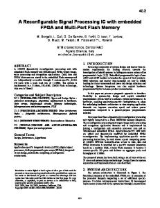
A Reconfigurable Instruction Memory Hierarchy for Embedded Systems† Zhiguo Ge1 , Hock Beng Lim2 , Weng Fai Wong1,2 1 Department of Computer Science, National University of Singapore. 2 Singapore-Massachusetts Institute of Technology Alliance, National University of Singapore. {gezhiguo,limhb,wongwf}@comp.nus.edu.sg
Abstract The performance of the instruction memory hierarchy is of crucial importance in embedded systems. In this paper, we propose a reconfigurable instruction memory hierarchy for embedded systems whose architectural parameters can be customized for specific applications. The proposed instruction memory hierarchy consists of an instruction cache and a scratchpad memory (SPM). We propose an algorithm to manage this instruction memory hierarchy and optimize its performance. Given a fixed amount of reconfigurable on-chip storage resources and an application, our algorithm determines the sizes of the SPM and the instruction cache to best suit the application. It analyzes the application, partitions the available storage resources into SPM and cache, and assigns instructions to them. Our algorithm aims to reduce the instruction fetch miss rate, improve the system performance, and reduce the energy consumption. We have implemented this reconfigurable instruction memory hierarchy on the Altera Nios II FPGA platform. Our experimental results using five benchmarks from the MediaBench and the MiBench suites show that our proposed architecture provides significant performance improvements and energy reduction.
1. INTRODUCTION The memory hierarchy is the main bottleneck in modern computer systems, due to the ever increasing gap between the speed of the processor and that of the memory. This problem becomes even worse in embedded systems, as designers not only need to consider performance, but also energy consumption. The memory hierarchy consumes a large amount of chip area and energy, which are precious resources in embedded systems. † This research was partially funded under the Singapore Agency for Science, Technology and Research (A*STAR) Project 022/106/0043.
Customizing the memory hierarchy [1, 2] for specific applications is an important way to fully exploit the limited resources to maximize the performance. Reconfigurable logic resources are being used for customizing the hardware platform for specific applications. In traditional hardwaresoftware co-design methodologies, much of the work have focused on utilizing reconfigurable logic to partition the computation. However, utilizing reconfigurable logic in memory hierarchy design is seldom addressed. The density and complexity of reconfigurable devices have been increasing dramatically. With the large amount of resources available, it is possible to design an embedded system using single FPGA chip. Software-core processors have been developed for FPGAs, such as the Altera Nios II and the Xilinx MicroBlaze. Our work focuses on exploiting reconfigurable logic to improve the performance of the instruction memory hierarchy for specific applications. We propose a reconfigurable instruction memory hierarchy consisting of an instruction cache and a scratchpad memory. The concept of scratchpad memory (SPM) [3] is an important consideration in embedded systems. Unlike the cache where the data replacement is controlled by hardware, the SPM is controlled by applications. Using SPM has the following advantages. First, the software-controlled SPM is more flexible and is able to avoid many cache conflicts. Second, since the SPM does not have tag, it consumes less hardware resource and energy than a cache. Given a fixed amount of reconfigurable on-chip logic resources and a specific application, we address the problem of partitioning the available resources into a SPM and an instruction cache, whose sizes depend on the application. Our goal is to lower the instruction fetch miss rate, improve the system performance, and to conserve energy. In this paper, we propose a reconfigurable instruction memory hierarchy for FPGA-based systems and an algorithm to explore the design space as well as perform instruction partitioning. To our knowledge, the design space exploration problem of partitioning a fixed amount of reconfigurable resources into an instruction memory hierar-
chy consisting of a SPM and a cache has not been addressed in the literature. Second, we have completed a prototype implementation of the proposed instruction memory hierarchy using actual FPGA hardware; namely, the Altera Nios II platform. We evaluated the performance of our proposed instruction memory hierarchy compared to one that consists of only an instruction cache. Using five benchmarks from the MediaBench and MiBench suites as workload, the experimental results show that our architecture provides significant performance improvements and energy reduction. The rest of the paper is organized as follows. In Section 2, we will discuss the related works and our contributions. Section 3 introduces the architecture of our proposed instruction memory hierarchy. We present the algorithm for design space exploration and instruction partitioning in Section 4. In Section 5, we discuss our prototype implementation using the Altera Nios II platform, the experimental methodology, and the results. We conclude this paper in Section 6. 2. RELATED WORK AND CONTRIBUTIONS The rationale and benefits of reconfigurable cache memory architectures have been well studied by previous researchers [4, 5]. There were also previous work to study the benefits of the SPM and to develop techniques to manage the SPM. Several researchers [6, 7, 8, 9] designed algorithms to partition instructions or data into the SPM, with the goal of reducing the conflict misses and the energy consumption. However, most of them assumed that the memory hierarchy has a fixed-size cache and a SPM, and they did not optimize the architectural parameters of the memory hierarchy. For example, Panda [8] partitioned the data objects in an application into the SPM and the cache to reduce the amount of cache conflicts. But he only considered two fixed memory hierarchy configurations; namely, a 2 KByte cache compared with a combination of 1 KByte cache plus 1 KByte SPM. Kandemir’s algorithm [9] can tune the size of the SPM, but it was designed for data references instead of instruction accesses. Vander et al [10] focused on adjusting the size of the instruction loop buffer for specific applications to maximize the energy savings. However, the cache is fixed and the problem they studied is different with ours. Apart from partitioning instructions into the SPM, some complementary techniques to optimize the performance of the instruction memory hierarchy are code positioning and mapping [11, 12, 13]. These techniques were developed to decrease the instruction cache miss rate by repositioning instruction blocks or procedures in the main memory. Our work differs from the previous work and is novel in two important ways. First, we focus not only on partition-
ing the instructions into the SPM, but also also on tuning the parameters of the memory hierarchy for specific applications. For a given amount of hardware resource budget for the instruction memory hierarchy, our algorithm partitions it into a SPM and an instruction cache. Our algorithm also assigns the instructions into the SPM by analyzing the instruction access characteristics of the specific application. Second, unlike previous work which rely mainly on simulations to evaluate the techniques for improving the performance of reconfigurable architectures, we have actually implemented our reconfigurable instruction memory hierarchy using real FPGA hardware. 3. DESIGN FLOW AND HARDWARE ARCHITECTURE 3.1. Design Flow The design flow for our reconfigurable memory hierarchy is shown in Figure 1. The inputs are the application and the hardware resource budget for the instruction memory hierarchy. The outputs are the transformed binary code, and the parameterized instruction memory hierarchy consisting of a SPM and an instruction cache of a certain size. Program
profile program
On-chip storage resource size
Perform partitioning on-chip storage resources into instruction cache and scratch memory and assign the instructions into the scratch and the cache Transformed Program
Instruction memory hierarchy with certain size of scratch and cache
Fig. 1. Design flow for the reconfigurable instruction memory hierarchy
The design process is as follows. First, we profile the application using the GCC compiler. Then, we compile the application into assembly code using the GCC cross compiler for the Nios II processor. From the assembly code, we build the data structure representations for our algorithm. These are then analyzed to determine the sizes of the SPM and the cache, as well as to partition the instructions into the SPM and the cache. We then patch the code that are allocated to the SPM to get the transformed assembly code. The transformed assembly code will be compiled using the GCC cross compiler for the Nios II to generate the binary executable. Finally, the parameterized instruction memory hieararchy coupled with the Nios II based system is compiled into FPGA using the Altera QuartusII tool.
Main
Load_instr_block
Addr
Sub-graphs in the second iteration
…
CPU Core
Addr_pre
Procedures
Load_instr_num Addr
Loops
Sub-graphs in the first iteration
60 slice
Hit
Address Lookup
60
Data
SPM controller
SPM_hit
1320
1289 Decode_macroblock
Motion_compensation 1320
Cache_hit Data
Instruction Cache
Data
2267 Decode_MPEG1_nonIntra_Block
SPM Addr
7920
Addr
7920 Add Block 7920
Fast_IDCT Cache miss
Load_instr_SPM
7920
7920
Data
63360
idctrow
63360 idctcol
29034 29034 26828 Get_Bits 49897 Flush buffer Show_Bits
Clear_Blcok
49897
514800
SDRAM
Fig. 2. The architecture of the reconfigurable instruction memory hierarchy
3.2. Instruction Memory Hierarchy Architecture The architecture of our reconfigurable memory hierarchy is shown in Figure 2. The memory hierarchy consists of an instruction cache, a SPM, a SPM controller (SPMC), an address lookup function unit (ALFU) and some other logic components. The ALFU is responsible for deciding whether an instruction resides in the SPM or not. It consists of two address registers and two parallel comparators. The two registers store the upperbound and the lowerbound addresses for the instruction block to be stored in the SPM. The highest and lowest instruction addresses of the block are stored in the upperbound and lowerbound register respectively. If the address of an instruction to be fetched falls within the range of these two registers, the ALFU will generate the signal SPM hit, which is used to control the selection and the switching of the cache and the SPM. The SPMC is used to load the instructions from the main memory into the SPM, and updating the values of the upperbound and lowerbound registers. Since the instructions are statically assigned into the SPM, the SPMC is actually optional. We can remove the SPMC from the memory hierarchy to save the resource usage. The instruction memory hierarchy is integrated in the Nios II processor. It is implemented in the form of a Verilog description. The sizes of the SPM and the cache are parameterized, and the parameters can be easily changed in the Verilog source code. 4. DESIGN SPACE EXPLORATION AND INSTRUCTION PARTITIONING A key aspect of our proposed instruction memory hierarchy is our algorithm for design space exploration and in-
Fig. 3. The Loop-Procedure Hierarchy Graph from mpeg2decode
struction partitioning. The design space exploration is to decide the sizes of the SPM and the instruction cache for an application, while the instruction partitioning is to assign the instructions into the SPM and the cache to maximize the performance and minimize the energy consumption. 4.1. Loop-Procedure Hierarchy Graph Our algorithm uses the Loop-Procedure Hierarchy Graph (LPHG) [14] to represent a program. Figure 3 shows the LPHG representation of a key portion of the mpeg2decode benchmark from the MediaBench suite. For simplicity, not all of the procedures and loops in mpeg2decode are shown. In this graph, the rectangular nodes represent the procedures, while the elliptical nodes represent the loops. The arrows (or edges) between the nodes denote the relationship between them. We call the node pointed to by an arrow a successor, while the node that points to another node is a predecessor. The numerical value associated with each arrow is the number times the successor is entered from the predecessor. 4.2. Proposed Algorithm The proposed algorithm is shown in Algorithm 1. We assume that most of the instruction cache conflicts are caused by the loops. The intuition is to put as many instructions from the frequently executed loop kernels into the SPM without causing severe cache conflicts for each important loop. We assume partitioning instructions is beneficial unless severe cache misses are incurred within one of those important loops. Starting with a storage resource of size M to be partitioned into the SPM and the cache, we divide this partitionable storage into two portions of size M/2 each. We will try to fill up one of these portions with instructions for
the SPM. Then, we recursively partition the other portion until the size of the remaining storage is so small that if it were to be further partitioned, there will be a large amount of cache conflicts when executing a kernel. Definition 1: a subgraph spanned by the loop L, denoted by SubG(L), is the subgraph consisting of all the nodes that are reachable from the loop node L. The size of a SubG(L), denoted by Sizeof(SubG(L)), is the number of instructions in the SubG(L) whose execution frequency in the loop exceed a certain threshold value, denoted as ExF reqT h. The idea is that within the SubG(L), there are certain instructions that are executed more frequently than others, and will be considered for placement in the SPM. In this paper, we set the ExF reqT h value to be 1/3 of the number of iterations in loop L. The algorithm starts from the leaf loops of the LPHG and work upwards during the course of its execution. This is because the deeper the loops are in the LPHG, the more frequently their instructions are executed. So, these loops should be assigned to the SPM. However, as we move to the upper levels of the LPHG, two or more SubGs at the level might be in conflict. Definition 2: Two SubG(L1) and SubG(L2) are in potential conflict if L1 and L2 are not a successor of each other. Given a partitionable storage of size M, SubG(L1) and SubG(L2) are in conflict if • SubG(L1) and SubG(L2) are in potential conflict • Sizeof(SubG(L1)) > M/2 and Sizeof(SubG(L2)) > M/2 At a particular level of SubGs, if no pair of SubGs are in conflict, then half of the partitionable storage should be added to the SPM. The instructions are then assigned to the SPM according to a calculated heuristic value. This process is repeated recursively with the remaining storage as the algorithm moves up the LPHG, until at least two SubGs at a particular level are in conflict. The instruction partitioning granularity is at the loop and procedure level. In line 8 of Algorithm 1, in a SubG, the frequently executed instructions in the loops and procedures will be selected to form the instruction blocks. The criteria to select the instructions is that the execution frequency of the instructions should be larger than ExF reqT h. The heuristic value for the selection of instruction blocks is computed in line 9 of Algorithm 1. We set the heuristic value as: Vh = Eavg + 5∗N umber of times called in this paper. Eavg is the average instruction execution frequency of a selected block, while N umber of times called stands for the number of the times the procedure containing the instruction block is called. Next, in line 10, the unimportant SubGs will be pruned from the list of SubGs. If a SubG’s Eavg is less than 1/20 of the average execution frequency of all the selected instruction blocks, we regard it to be unimportant and will not consider it in the current iteration.
Algorithm 1 Design space exploration and instruction partitioning 1: 2:
INPUT: Assembly code and source code profiling information, storage size M OUTPUT: The SPM size and the assignment of instructions into SPM
3: 4: 5: 6: 7: 8: 9: 10: 11: 12: 13: 14: 15: 16: 17: 18: 19: 20: 21: 22: 23: 24: 25: 26: 27: 28: 29: 30:
Variable P M : current partitionable storage size Build Loop-Procedure Hierarchy Graph(LPHG) PM = M; while (P M > Lower Bound of Cache Size) do Select the instruction blocks for loops and procedures in SubGs list; Calculate the heuristic value, Vh , for all the selected instruction blocks; Prune the non-important SubGs; if (!two SubGs conflict(SubGs list, PM) then Select instruction blocks from SubGs until P M/2 amount of storage is filled; P M = P M/2; goto Update; else // there is a conflict between at least two SubGs. break; // break the while loop end if Update: Update SubGs list; end while Cache size = P M , SPM size = M - Cache Size; Pack all the extracted instruction blocks into the SPM with the determined size; return; Procedure two SubGs conflict(SubGs list, PM) if (size of all SubGs in the SubGs list is smaller than PM/2) then return false else if (size of only one graph in the SubGs list is larger than PM/2) then return two SubGs conflict(list of all the child SubGs in the current SubG, PM); else return true; end if
In our algorithm, the procedure two SubGs conf lict is used to determine whether there exists two SubGs in the list of SubGs which are in conflict. If two SubGs are in conflict, which means their sizes are larger than P M/2, further partitioning the current partitionable storage into the SPM and the cache is likely to cause more cache conflicts. Thus, we stop the partitioning process. On the other hand, if none of the SubGs are in conflict, we can assign P M/2 amount of storage to the SPM. Then,
we select the instruction blocks from the list of SubGs to fill the P M/2 amount of storage in the SPM according to the heuristic value, Vh . Once the SPM is filled, the list of SubGs will be updated and the process repeats. Apart from the detection of conflicts between SubGs, another termination criteria of the algorithm is that the remaining storage for the cache should not be lower than a threshold value, Lower Bound of Cache Size. In the mpeg2decode example in Figure 3, the SubG list initially contains all the leaf SubGs in the LPHG. From the figure, all the SubGs in dashed boxes are in the SubGs list of the first iteration, while the SubGs in the hemispheres are in the SubGs list of the second iteration. For mpeg2decode, the given on-chip storage is 2048 bytes. The size of every SubG in the first iteration is less than 1024 bytes. Thus we can partition the half the storage into the SPM. After assigning the instructions into the SPM, the SubGs list will be updated and the second iteration starts. However, the algorithm terminates at the second iteration because the size of both the SubGs (shown in the hemispheres in Figure 3) in the SubGs list are larger than 512 bytes. Thus, the final memory hierarchy configuration consists of 1024 bytes of instruction cache and 1024 bytes of SPM. 5. PERFORMANCE EVALUATION
Table 1. Performance results Benchmk Configs
Nf (K)
g721encode Improv
2048C 512C+1536S
195,124 − 196,057 82.2
−
−
g721decode Improv
2048C 512C+1536S
293,637 − 299,005 86.0
−
−
−
Dijkstra
256C 64C+192S
48,582 49,789
− 73.2
Improv
−
−
−
25,617 25,621
− 94.6
−
Blowfish 2048C 64C+1984S Improv − mpeg2decode Improv
2048C 38,532 1024C+1024S 38,567
−
Avg Impr −
− −
RS (%) miss(%) Te (sec) 3.09 1.93 37.5%
6.14 5.45 11.2%
2.51 1.35 46.2%
9.16 8.15 11.0%
2.06 1.93 6.3%
2.24 2.24 0.0%
−
2.21 0.67 69.7%
0.85 0.74 12.9%
− 51.9 −
1.44 1.35 6.3%
1.46 1.45 0.7%
−
33.2%
7.2%
−
since it is not active once instructions are loaded, as we explained in Section 3.2. We assume that the row activation and precharge of the SDRAM consumes 20nJ, while column access consumes 26nJ [16].
5.1. Experimental Methodology 5.2. Performance Improvements and Energy Savings We used the Nios II Development Kit (Stratix Edition) as our development platform. We implemented the reconfigurable memory hierarchy shown in Figure 2 by modifying the Nios II Verilog source code. The cache is directmapped, with line size of 32 bytes. Hardware counters are added to the system to collect the program execution statistics, such as the number of cache misses, the number of instruction fetches, the number of issued instructions, and the total number of cycles taken. We then synthesized the system using the QuartusII tool. In our experiments, we used five application benchmarks from the MediaBench and the MiBench suites. We compared the performance and the energy consumption of executing each benchmark on two different instruction memory hierarchies: (1) a baseline instruction memory hierarchy with only an instruction cache, and (2) our instruction memory hierarchy combining a SPM and an instruction cache. We executed these benchmarks and collected the performance statistics from the hardware counters. We modelled the energy consumption using the CACTI [15] model for 0.5 µm technology. In the calculation of the energy consumption of our instruction memory hierarchy, we included the logic elements connecting the instruction cache and the SPM to the Nios II processor. However, we excluded the SPMC from the energy consumption calculation
Performance: The performance results are shown in Table 1. Nf (K) is the total number of instructions fetched (in thousands), and RS (%) stands for the percentage of the number of instruction fetches from the SPM out of the total number of instruction fetched. The miss(%) is the miss rate of the instruction fetching. Te (sec) is the application execution time in seconds. The baseline configuration of ”2048C” is an 2048-byte instruction cache. For our instruction memory hierarchy, ”1024C+1024S” in mpeg2decode means a 1024-byte cache and a 1024-byte SPM. From the results, the decrease in the instruction fetch miss rate for the benchmarks studied ranges from 6.3% to 69.7%. The average improvement in the miss rate is 33.2%. This improvement in the instruction fetch miss rate for our instruction memory hierarchy over the baseline cache configuration comes from the mapping of the frequently executed instructions into the SPM. As a result of the improvement in miss rate, the execution times of the applications are decreased by an average of 7.2% for the benchmarks studied. The improvement in execution time is not as impressive as the improvement in miss rate. A possible reason is that due to the low clock frequency (50M Hz) of the hardware platform, the cache miss penalty becomes less important.
Multimedia System Design.
Table 2. Energy consumption EC
Benchmk Configs
EC
ES
ET ot (µJ) Rd(%)
(nJ) (nJ) (nJ) g721encode g721decode Dijkstra
2048C 512C+1536S 2048C 512C+1536S 256C 64C+192S Blowfish 2048C 64C+1984S mpeg2- 2048C decode 1024C+1024S Avg Rd
−
1.51 − 1.51 − 1.09 − 1.51 − 1.51 −
− 1.33 − 1.33 − 1.10 − 1.10 − 1.41
− 1.12 − 1.12 − 0.83 − 1.19 − 1.04
1,669,325 1,089,642 2,123,818 1,264,014 281,134 258,543 161,386 69,534 184,691 165,683
−
−
−
−
34.7% 40.5% 8.0% 56.9% 10.3% 30.1%
Energy consumption: The energy consumption results are shown in Table 2. EC (nJ) represents the energy consumption per access to the instruction cache, while ES (nJ) is the energy consumption per access to the SPM. We computed the total energy consumption (ET ot (µJ)) during the execution of the benchmark for the two instruction memory hierarchies, as well as the reduction in the energy consumption (Rd(%)) due to our instruction memory hierarchy. From the results, the reduction in the energy consumption for the benchmarks studied ranges from 8.0% to 56.9%. The average reduction in the energy consumption is 30.1%. A major contribution to the energy reduction is the decrease in miss rate since SDRAM accesses consume a lot of energy. The other factor that results in the energy reduction is the lower energy consumption per access to the SPM compared to that of the cache, and most instruction fetches are from the SPM. 6. CONCLUSION We have designed a reconfigurable instruction memory hierarchy for embedded systems. Given a fixed amount of on-chip storage and a specific application, our algorithm partitions the storage into a SPM and an instruction cache, and assigns instructions to the SPM and the cache to maximize the performance and reduce the energy consumption. We believe that our approach is novel because previous work are not as flexible in their design space exploration of the instruction memory hierarchy. Experimental results show that our proposed architecture can achieve significant performance improvements and energy reduction. 7. REFERENCES [1] F. Catthoor, et. al., Custom Memory Management Methodology: Exploration of Memory Organization for Embedded
Kluwer, 1998.
[2] P. R. Panda, N. Dutt, and A. Nicolau, Memory Issue in Embedded Systems-on-chip: Optimization and Exploration. Kluwer, 1999. [3] R. Babakar, et. al, “Scratchpad memory: A design alternative for cache on-chip memory in embedded systems,” in Proc. 10th Intl. Symp. on Hardware/Software Codesign (CODES ’02), May 2002, pp. 73–78. [4] P. Ranganathan, S. Adve, and N. P. Jouppi, “Reconfigurable caches and their application to media processing,” in Proc. 27th Intl. Symp. on Comp. Arch. (ISCA-27), June 2000, pp. 214–224. [5] C. Zhang, F. Vahid, and W. Najjar, “A highly configurable cache architecture for embedded systems,” in Proc. 30th Intl. Symp. on Comp. Arch. (ISCA-30), June 2003, pp. 136–146. [6] M. Verma, L. Wehmeyer, and P. Marwedel, “Cache-aware scratchpad allocation algorithm,” in Proc. 2004 Design, Automation and Test in Europe Conf. (DATE ’04), Feb. 2004, pp. 21 264–21 269. [7] S. Steinke, et. al., “Assigning program and data objects to scatchpad for energy reduction,” in Proc. 2002 Design, Automation and Test in Europe Conf. (DATE ’02), Mar. 2002, pp. 409–416. [8] P. R. Panda, N. Dutt, and A. Nicolau, “On-chip vs. offchip memory: The data partitioning problem in embedded processor-based systems,” ACM Trans. on Design Automation of Elect. Sys., vol. 5, no. 3, pp. 682–704, July 2000. [9] M. Kandemir and A. Choudhary, “Compiler-directed scratch pad memory hierarchy design and management,” in Proc. 39th Design Automation Conf. (DAC ’02), June 2002, pp. 628–633. [10] T. V. Aa, et. al., “Instruction buffering exploration for low energy embedded processors,” in Proc. 13th Intl Workshop on Power And Timing Model., Optim. and Simul., Sept. 2003. [11] K. Pettis and R. C. Hansen, “Profiling guided code positioning,” in Proc. 1990 Conf. on Prog. Lang. Design and Imple. (PLDI ’90), June 1990, pp. 16–27. [12] A. H. Hashemi, D. R. Kaeli, and B. Calder, “Efficient procedure mapping using cache line coloring,” in Proc. 1997 Conf. on Prog. Lang. Design and Imple. (PLDI ’97), June 1997, pp. 171–182. [13] N. Gloy, et. al., “Procedure placement using temporal ordering information,” in Proc. 30th Intl. Symp. on Microarch. (Micro-30), Dec. 1997, pp. 303–313. [14] Y. Li, et. al., “Hardware-software co-design of embedded reconfigurable architectures,” in Proc. 37th Design Automation Conf. (DAC ’00), June 2000, pp. 507–512. [15] S. J. E. Wilton and N. P. Jouppi, “CACTI: An enhanced cache access and cycle time model,” IEEE Journal of SolidState Circuits, vol. 31, no. 5, pp. 677–688, May 1996. [16] Y. Han, http://www.ece.neu.edu/groups/nucar/barc2004/ BARC2004-yhan.pdf, 2004.