A Low-Noise, Low-Power EEG Acquisition Node for Scalable Brain-Machine Interfaces Thomas J. Sullivana and Stephen R. Deissa and Gert Cauwenberghsa and Tzyy-Ping Jungb,c a Department
b Institute for Neural Computation of Biology University of California, San Diego, 9500 Gilman Dr., La Jolla, California, USA c National
Chiao Tung University 1001 Ta Hsueh Road, Hsinchu, Taiwan ABSTRACT Electroencephalograph (EEG) recording systems offer a versatile, non-invasive window on the brain’s spatiotemporal activity for many neuroscience and clinical applications. Our research aims at improving the spatial resolution and mobility of EEG recording by reducing the form factor, power drain and signal fanout of the EEG acquisition node in a scalable sensor array architecture. We present such a node integrated onto a dimesized circuit board that contains a sensor’s complete signal processing front-end, including amplifier, filters, and analog-to-digital conversion. A daisy-chain configuration between boards with bit-serial output reduces the wiring needed. The circuit’s low power consumption of 423 µW supports EEG systems with hundreds of electrodes to operate from small batteries for many hours. Coupling between the bit-serial output and the highly sensitive analog input due to dense integration of analog and digital functions on the circuit board results in a deterministic noise component in the output, larger than the intrinsic sensor and circuit noise. With software correction of this noise contribution, the system achieves an input-referred noise of 0.277 µVrms in the signal band of 1 to 100 Hz, comparable to the best medical-grade systems in use. A chain of seven nodes using EEG dry electrodes created in micro-electrical-mechanical system (MEMS) technology is demonstrated in a real-world setting. Keywords: EEG, brain-computer interface, brain-machine interface, biosensor
1. INTRODUCTION Electroencephalograph (EEG) systems designed for use on humans record electrical potentials from various locations on the scalp. These potentials are generated by neural activity within the brain and may ultimately shed light on the inner workings of the brain. The EEG sensors are typically made of metal and make contact with the skin through an electrically-conductive gel. The sensors (also called electrodes) are mounted on a cap that the subject wears on the head. These systems have many research and clinical applications.4, 5 Two issues limit the use of these systems. The first is that electrically-conductive gel is required for a good connection between the sensors and the scalp. This gel takes a lot of time to apply, it limits the realizable density of sensors on the scalp, and it tends to dry out, which limits the recording time. Efforts are currently underway to alleviate these issues by creating MEMS sensors that do not require gel.2 The second limiting issue with typical EEG systems is that they are not portable. The EEG cap is not portable due to the mass of wires connecting the cap to the data-collecting computer, as well as high power consumption. This is the problem we address here. The circuit described is intended to provide all the analog signal processing for one electrode. The number of wires needed to interface with a large number of electrodes will be reduced since the power, clocks, and measured signals are daisy-chained from one board to another. If all the data are concatenated at each measurement time, then only a couple wires, or a wireless interface, will be sufficient to send the data to a computer for recording. Also, with 256 of these signal processing boards, less than 40 mA would be consumed with a 3V supply. Three rechargeable AAA NiMH batteries with a 900 mAh capacity would be able to power the entire EEG recording system for several hours. Send correspondence to T.J.S. by E-mail:
[email protected]
2. CIRCUIT DESIGN The analog front-end circuit is shown in Figure 1. It consists entirely of off-the-shelf components, which keeps the overall system cost low. The circuit amplifies the incoming EEG signal, filters out frequencies that are not in the band of interest, and digitizes the signal. The LT6010 operational √ amplifier was chosen for the amplification because it provides a good trade-off between low noise (14 nV/ Hz voltage noise density with a low 1/f knee) and low current consumption (130 µA). It is configured for a mid-band gain of 1000. A 100 µF capacitor is used to cut the gain to 1 at frequencies below 1 Hz. This is important since the sensor/scalp interface often generates significant DC offset voltages up to 25 mV. This offset voltage would saturate the output of the amplifier if it weren’t filtered to a unity-gain level. A capacitor in the feedback path, C1, creates a low-pass filter with a -3dB cutoff at 100 Hz. A second pole is set up at 1 kHz by R2 and C3. After the filters the voltage is sampled at 2 kS/s by the LTC7691 analog-to-digital converter (ADC). This ADC was chosen for several reasons: (1) it can convert at an 18-bit resolution, so it will not contribute a significant amount of quantization noise, (2) it consumes less than 20 µA of current at 2 kS/s, and (3) it comes with the option of daisy-chaining the output (this advantage will be discussed later). While EEG signals generally do not extend beyond 100 Hz, noise from muscle movements is often found in frequencies up to 1 kHz. The signals in this band are digitized because this muscle noise may be a valuable signal for researchers doing EEG experiments in which the subjects are moving around and interacting with the world. The electrode connects directly with the high-impedance, non-inverting input of the amplifier. The idea was to load the sensor as little as possible. One feature of this configuration is that the DC voltage level from the electrode appears at the output with a unity gain. In practice, the offset voltage is used to determine if a good connection is being made with the scalp. Voltages less than an absolute value of 25 mV are typical for good connections, while poor connections will result in voltages that float to larger voltages. Thus, with this configuration it is possible to read the DC level of the output voltage and determine with some confidence if a good connection is being made. This DC level can be easily subtracted by software once data from the sensors is recorded. The circuit was built on a custom PC board (see Figure 2, Top). The circuit is roughly the size of a dime. The signal is connected to the sensor with a pin extending from the bottom of the board in the center. The two ICs are in MSOP and DFN packages. The passive components are all in 0603 packages (measuring 60 mils by 30 mils) except for the large 100 µF capacitor, which can be seen at the top toward the middle of the circuit. The
Figure 1. Analog Front-end Schematic. The circuit consists of an off-the-shelf amplifier and analog-to-digital converter. The mid-band gain is 1000 with noise filtered out below 1 Hz and above 100 Hz.
two big structure on the left and right edges are connectors. They connect to other EEG sensor circuit boards. These connections serve two purposes: (1) to share the power, reference voltage, and ADC clocks, and (2) to daisy chain the digital outputs. Configuring boards into a daisy chain means that the output of one circuit will be passed to another board. All the outputs are, in effect, concatenated into one long serial bit-stream and read by the data acquisition system. When many electrodes are used on one EEG cap (256, for example) passing all these signals from one board to another drastically reduces the number of wires that are required for control and read-out.
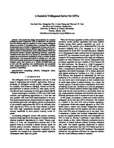
Figure 2. Photographs of EEG System. (Top) The analog front-end circuit for one EEG sensor was built on a custom miniature PC board. The small size will allow for 256 electrodes or more to fit onto a standard sized EEG cap. (BottomLeft) Seven electrode circuits are mounted onto a baseball cap. This is not a traditional approach to building EEG recording devices, but may be feasible with the latest dry sensors. (Bottom-Right) The dry sensors are mounted onto the inside brim of the baseball cap to get EEG readings from the forehead of the subject. Each sensor measures 4x4 mm.
3. CIRCUIT PERFORMANCE 3.1. Gain and Phase Response The gain and phase responses of the amplifier section of the circuit were measured with a lock-in amplifier.6 Using this instrument, the frequency of a pure sine wave, used as an input signal, was swept across the spectrum. The gain and the phase of the resulting output are shown in Figure 3. The mid-band gain is 60 dB (or 1000) and falls off below 1 Hz and above 100 Hz. Since the measurement was taken at the amplifier output, the second pole (which kicks in at 1 kHz) is not a factor.
Amplifier Gain (dB)
70 60 50 40 30 20 10 0 −2 10
−1
10
0
10
1
10
2
10
3
10
4
10
5
10
Output Phase (Deg.)
Frequency (Hz) 90 45 0 −45 −90 −2
10
−1
10
0
10
1
10
2
10
3
10
4
10
5
10
Frequency (Hz)
Figure 3. Gain and Phase Response. The gain and phase response were measured at the output of the operational amplifier. (Top) The gain is 60 dB (or 1000) in the signal band of 1 Hz to 100 Hz. (Bottom) The output phase ranges from +45 degrees to -45 degrees in the signal band.
An example of the output of the amplifier when driven by a sine wave is shown in Figure 4. The input was generated with the output of a function generator driven into a 20,000 to 1 resistor voltage divider. This was necessary in order to get a sine wave with a very small amplitude. In this case the peak-to-peak amplitude is 85 µV with a frequency of 10 Hz, which is in the range of typical EEG signals. In the figure, the DC amplitude has been removed and the voltage has been input-referred by dividing by the amplifier gain.
3.2. Common-mode Rejection In order to test the common-mode rejection, the sensor input and reference voltage were tied together. A function generator was used to drive this node with sine waves of various frequencies. The results are shown in Table 1. As expected, the common-mode gain is close to 1 in the signal band and at low frequencies. The common-mode signal is not gained up or filtered by the amplifier configuration. The common-mode rejection is obtained by dividing the signal gain by the common-mode gain. It is 60 dB in the signal band. This should be good enough to reject in-band noise, including 60 Hz power line noise. The output of the circuit when driven by an example 60 Hz common-mode signal is shown in Figure 5. The DC level of the output has been removed for clarity. The input amplitude was 200 mVpp and it feeds through with a slight attenuation.
Input−referred voltage (uV)
60 40 20 0 −20 −40 −60 0
0.05
0.1
0.15
0.2
0.25
0.3
0.35
0.4
0.45
0.5
Time (sec)
Figure 4. Signal Response. A 10 Hz, 85 µVpp sine wave was used as an input and this waveform was recorded at the ADC output. This example is consistent with the gain vs. frequency curve.
Table 1. Common-mode Rejection
Frequency
Common-mode
Common-mode
Gain
Rejection (dB)
1
1.02
57
10
1.00
60
100
0.88
57
1,000
0.78
40
10,000
0.78
20
150
Output Voltage (mV)
100
50
0
−50
−100
−150 0
0.01
0.02
0.03
0.04
0.05
0.06
0.07
0.08
0.09
0.1
Time (sec)
Figure 5. Common-mode Response. A 60 Hz, 200 mVpp sine was was used as a common-mode input (with the sensor input and reference voltage tied together). The signal feeds through with a gain slightly less than 1, implying a commonmode rejection of 60 dB.
3.3. Noise and Coupling Cancellation The noise generated by the circuit was measured by connecting both the sensor input and the reference input to the same reference voltage at mid-supply. The digital output was recorded with a data-acquisition system for 20 seconds, then processed in Matlab. A digital low-pass filter was applied to the collected data with a steep cutoff at 100 Hz. The output of one electrode circuit was then subtracted from another (with the same input) in order to eliminate the common-mode noise. The maximum and minimum voltages were used to calculate the peak-to-peak voltage, and the root-mean-square (RMS) measure of the noise was calculated from the same data. When measuring the noise performance of the circuit an interesting phenomenon was observed. A typical output is shown on the top panel of Figure 6. The magnitude is much higher than anticipated. Additionally, it has some structure that should not be present in completely random white noise. It was determined that the most significant source of the coupling-induced digital noise comes from the transitions on the ADC output line. Each analog-to-digital conversion cycle is followed by 18 clock cycles that serially read out the result of the conversion. The clock signal used for this process is a 1.84 Mhz square wave with sharp edges. Digital noise generated by this clock signal and the ADC output contaminate the ground, power, and reference lines. In addition, an unknown amount of capacitive coupling may occur between the digital lines and the sensitive amplifier inputs. Exactly where this coupling occurs was not determined. The effect of the up and down output transitions at one point in time on the next analog voltage sample are predictable. Therefore, a simple model of this coupling was created in order to cancel it out. At each sample time, the noise-cancelation scheme simply adds up the total number of ADC output transitions between 0 and 3V. This total number, called s, is multiplied by a parameter, β, and subtracted from the analog voltage sampled at the next sample time. To obtain the parameter, a model was first constructed of the expected voltage output: vk+1 = αvk + βsk + γ + η
(1)
Here, vk is the measured voltage at time point k, α is a parameter that takes into account the fact that the voltage at one point in time will resemble the voltage at the previous time point (due to the low pass filtering), γ is the DC offset of the output, and η is the unpredictable random noise due to the circuit. Twenty seconds of data is taken and used in a linear regression to obtain the parameters. β is then used to cancel out the digital coupling. The results of this procedure are shown in the bottom panel of figure 6. The final noise is 0.277 µVrms (and 2.16 µVpp) in the signal band (1-100 Hz). In the bottom panel, there appears to be even more structure
Input−referred voltage (uV)
15
10
5
0
−5
−10
−15 0
0.1
0.2
0.3
0.4
0.5
0.6
0.7
0.8
0.9
1
0.6
0.7
0.8
0.9
1
Time (sec)
Input−referred voltage (uV)
15
10
5
0
−5
−10
−15 0
0.1
0.2
0.3
0.4
0.5
Time (sec)
Figure 6. Noise Cancellation. The ADC output is recorded with the sensor input and reference input tied to a reference voltage. (Top) The low-to-high and high-to-low transitions of the ADC output couple back to the signal. (Bottom) Software correction is applied to cancel out the coupling.
in the data, which should not be present in truly random noise. The noise-cancelation scheme most likely does not cancel out all the coupling. Future research efforts will address this point.
3.4. EEG Data A test was performed in which EEG data was taken from a person. The dry sensors (shown in Figure 2) were attached to the forehead and secured with tape. In one test, the subject was asked to blink his eyes in a specific pattern. The resulting EEG patterns are shown in the top panel of Figure 7 with the timing of the eye-blinks indicated with arrows. The deflections in the EEG voltage are typical of eye blinks. In another test, the subject was asked to keep his eyes open for 30 seconds, then closed for the next 30 seconds. A power spectral density was calculated from the data of each of the 30 second sessions. This is displayed in the bottom panel. A bump at 10 Hz (indicated by the arrow) is a result of increased α-waves with the eyes closed. This is a typical EEG signal which is currently being investigated by the brain research community.
4. DISCUSSION The purpose of this work is to improve the spatial resolution and mobility of EEG recording systems. The spatial resolution of EEG systems can be increased by using signals obtained from dry EEG sensors. This is because the commonly-used sensors employing electrically-conducive gel are limited to using a large amount of space so that the gel from neighboring sensors does not make a shorting contact. Our EEG acquisition node circuit is compatible with recently-invented MEMS sensors that do not require gel.2 Although, one nice feature of our board is that it can be used equally well with dry sensors or sensors that require gel. We address the need for mobility in EEG recording equipment by creating a daisy-chain of digital outputs consisting of all the electrode boards. This way, the wiring requirements for power, control, and read-out are reduced making a wireless solution more feasible. Also, mobility is possible because only a small amount of power is required for the whole signal processing system. Small batteries can be employed to power the system for an extended period of time. The sensor front-end circuit described here is suitable for implementation in a mobile EEG cap with many electrodes (256, for example). This would open up possibilities for entirely new types of experiments in which the subjects can move around and interact with the world. One can imagine many experimental settings that will be opened up, for example several people interacting naturally in a social environment, athletes performing in a sport, and movement-based meditation techniques. Surely there are even more new paradigms that could utilize mobile EEG devices that are yet to be explored.
ACKNOWLEDGEMENTS The authors would like to thank Ruey-Song Huang, Scott Makeig, Don Kimball and Ramesh Rao for help in facilitating the testing of this circuit. We would like to thank Ian Galton for useful discussions about the design and Dr. J.C. Chiou and the members of the National Chiao Tung University Brain Research Center for the use of their dry MEMS sensors. This work was supported by DARPA.
REFERENCES 1. BioSemi Company Website, http://www.biosemi.com. 2. J. C. Chiou, Li-Wei Ko, Chin-Teng Lin, Chao-Ting Hong, Tzyy-Ping Jung, “Using Novel MEMS EEG Sensors in Detecting Drowsiness Application,” IEEE Biomedical Circuits and Systems Conference, 2006. 3. R. R. Harrison, C. Cameron, “A low-power low-noise CMOS amplifier for neural recording applications,” IEEE Journal of Solid-State Circuits 38: 958-965, June 2003. 4. T. P. Jung, S. Makeig, M. Stensmo, and T. Sejnowski, “Estimating alertness from the EEG power spectrum,” IEEE Transactions on Biomedical Engineering 44:60-69, 1997. 5. J. Onton, A. Delorme, S. Makeig, “Frontal midline EEG dynamics during working memory,” NeuroImage 27:431-56, 2005. 6. SR830, Stanford Research Systems Website, http://www.thinksrs.com.
Scale 0.2 mV − +
1
0
2
4
6
8
10
12
14
16
18
20
22
24
26
28
30 (sec)
Power Spectral Density Estimate via Welch −30 Eyes opened Eyes closed
Power/frequency (dB/Hz )
−40
−50
−60
−70
−80
−90
0
10
20
30
40
50
60
Frequency (Hz)
Figure 7. EEG Signal Recorded from Live Subject. A typical recording is shown from one sensor on the forehead. (Top) EEG signal resulting from eye blinks. Arrows indicate times at which the subject blinked his eyes. (Bottom) The power spectral density of two 30-second sessions. During one session the subject kept his eyes open, during the other he closed his eyes. The characteristic bump at 10 Hz is a result of α-waves that typically appear when subjects close their eyes.